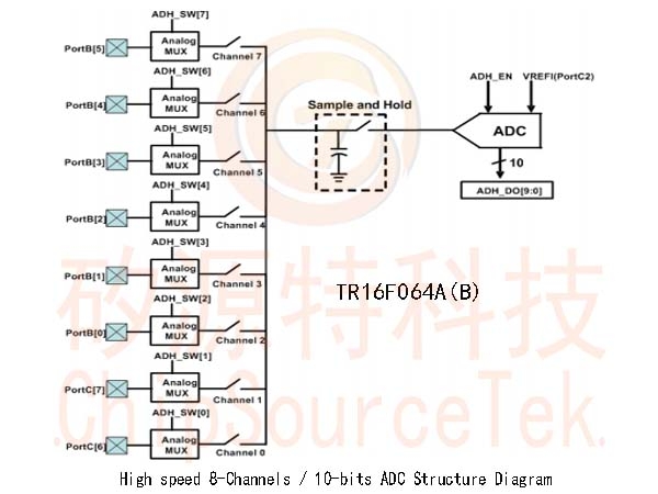
TR16F064A(B) General Description:
The TxP16ETM is a high performance 16-bit MCU, running up to 32MHz and provided with 64K FLASH and total 4K SRAM for high performance process of audio algorithm, power control and motor control. It is the new generation computational kernel for Flash DSP series. It has initially aimed at the areas of controller and multimedia digital signal processing (DSP) application to demonstrate its profession. TxP16E furnish with fast MAC architecture, which allows multiplication+accumulation instructions to be issued with access memory simultaneously during one cycles. The TR16F064 is equipped with TxP16E and integrating input/output ports,Audio PWM, Timer and Low Voltage Reset...etc on a chip. Built-in high-speed 10-bit ADC can apply to AC power and motor control application easily.
Furthermore, TR16F064 extend its external device connection capability such as Serial ROM/Flash. The internal memory capacity includes 64Kx16 program/data FLASH plus 4Kx16 working SRAM.
TR16F064A(B) Features:
High-performance RISC TxP16E CPU
*wide working frequency and voltage 1Mhz ~32Mhz@1.8Volt ~ 5.5Volt
*Operation frequency is programmable by Software
*Built-in 4096x16 SRAM
*Hybrid Instruction and data memory share with 64Kx16 Flash ROM
*Embedded PC Stack Level 24
Rich DSP function
*Hardware Circular Buffer support
*MAC Computation power : 32MIPS (max.)
*Multi-Function Support: In MAC calculation, simultaneously access two operands from memory in one cycle
*Extend Dynamic Range: A 40-bit accumulator to ensure in 512 successive multiple+additions no overflows
Embedded Flash 64Kx16
*Typical 100,000(TR16F064A) / 20,000(TR16F064B) erase/program cycles
*Greater than 10 years Data Retention
Software-based audio processing technical
*Subband, ADPCM , CELP , Melody systhesis up to 20 channels ( Max )
Support 20+2(ICE PAD can be as I/O) general purpose I/O port, can be configured to open-drain output
Stereo 8~ 16-bit PWM can be adjustable
15 IRQ & 1 NMI
*NMI is non-mask interrupt, can interrupt IRQ immediately
*2 external interrupt
4 bit SPI Master Hardware support DMA transfer
SPI Slaver
Green Mode
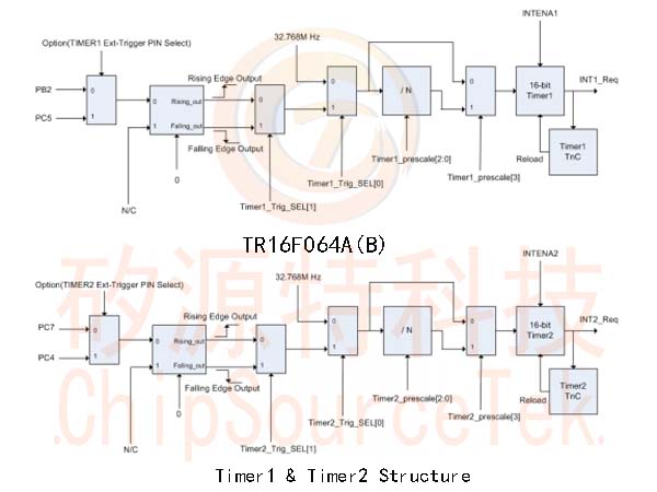
Timer1 , Timer2 with Pre-scale
Low power instruction
24-Hours / One day Real-Time Clock
ICE support Data RAM monitor for motor control debug
Support Spread Spectrum clocking to reduce EMI.
CPU Array
Watch dog timer (WDT)
Low voltage reset (LVR)
Low dropout regulator(LDO) supply 3.3V/1.8V@20mA (voltage drop 0.1v )
PB0, PB1, PB2, PB3 support two edge modes for wake-up function are rising and falling edge trigger.
Comparators
ADC 10bit / 285 kbps(@ACQT = 4*TAD) / 8 channel
Temp. Sensor
Microphone
1402 interface
TR16F064A(B)Application Field
MCU Application
Electronic Dictionary
Handheld Games
Electronic Learning Aid (ELA)
Digital Photo Frame
Electronics storybook
Power / motor control
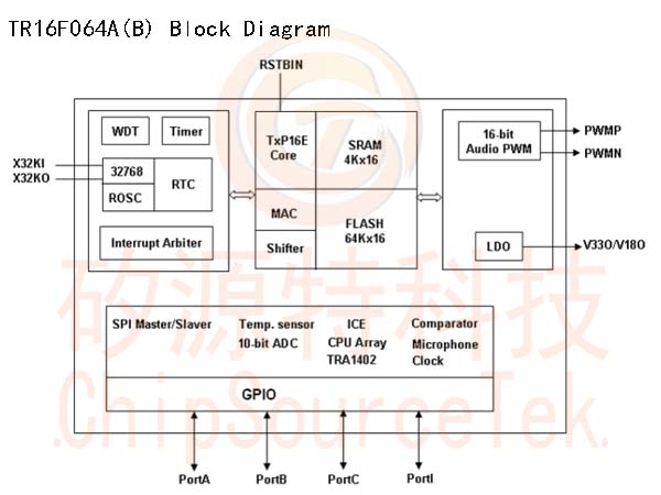
TR16F064A(B) Block Diagram:

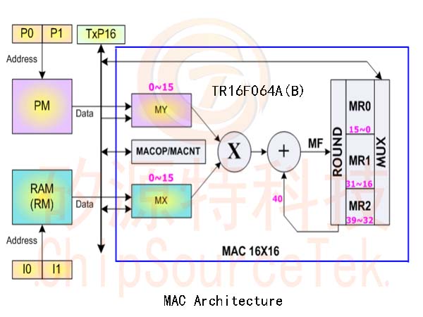
TR16F064A(B) MAC (16-bit X 16-bit Multiplier and Accumulator):
A 16 bit x 16 bit MAC is provided for digital signal processing. The core of MAC operation is multiply MX&MY
with 2’S complement operand and accumulation previous 40-bit MF then rounding store result in the 40-bit MR
register. The basic MAC architecture is shown as Figure.

TR16F064A(B) Timer1 & Timer2 Structure:
TR16F064A(B) High speed 8-Channels/10-bits ADC Structure Diagram:
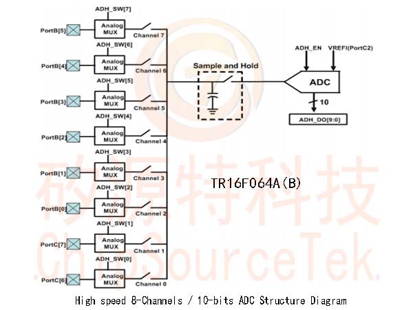
Note: If user need more precise ADC for application, user can use PortC2 as voltage-reference input(VREFI) of
ADC. Independent voltage-reference input pin can improve ADC precision.
Note: Enable ADC verf input at option, PortC2 is as ADC voltage-reference input(VREFI), not as I/O pin.
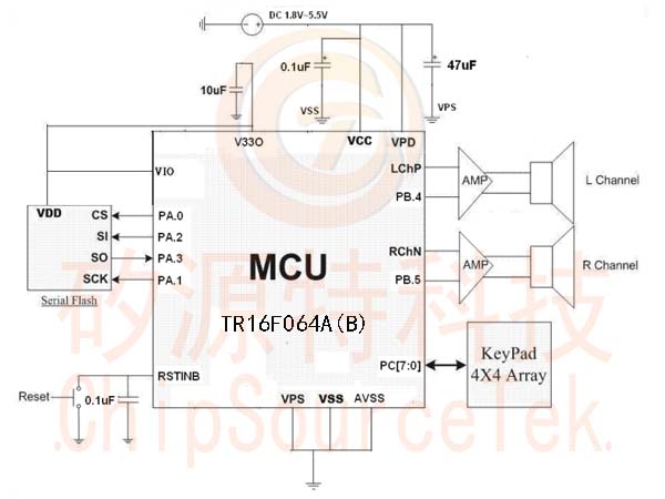
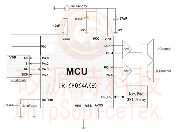
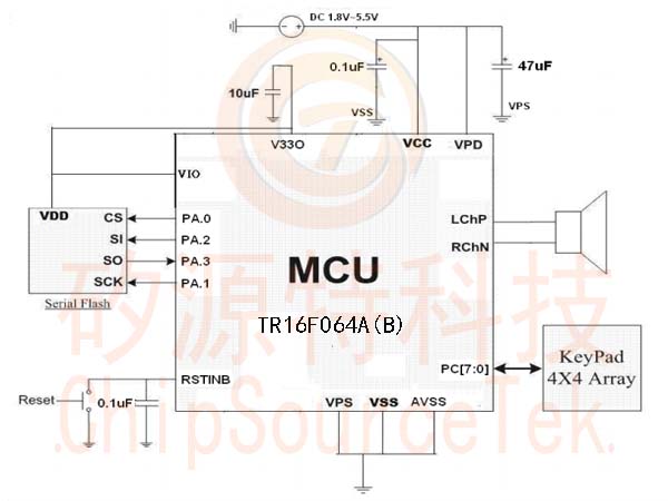
** The decouple capacitor (10uF) must be as near as possible to VCC and VSS.
TR16F064A(B) Application Circuit:

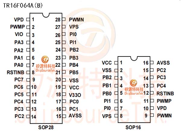
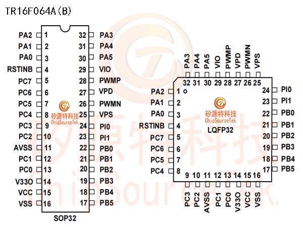
TR16F064A(B) Package: SOP28 / SOP32 / SOP16 / LQFP32:
