Trends in Hall effect current sensing
Time:2023-10-08
Views:630
This article introduces some progress in the use of Hall effect current sensor integrated circuits. This document contains various packaging concepts that incorporate the main current path into the system, major improvements to IC parameters, and some examples of typical application circuits for UPS, inverter, and battery monitoring.
introduce
Over the past decade, the demand for low-cost, small-scale current sensor solutions in industrial, automotive, commercial, and communication systems has rapidly increased. Various techniques can be used to convert current into proportional voltage. The advantages of Hall effect magnetic detectors are inherent voltage isolation from the current path and the integration of Hall elements and interface electronic devices on a single silicon chip. [1] The new design concept and the use of advanced BiCMOS technology in the system have further improved the performance of the IC. By supporting the integration of additional features such as power protection in the same current sensor IC, these also open the door to new product methods.
Packaging concept
The characteristic of Allegro current sensor IC devices is the integration of a single linear Hall IC and a low resistance primary current conduction path into a single injection molding package. Optimize equipment accuracy through the close proximity and positioning of Hall sensors relative to copper conductors. Low power consumption and high voltage isolation are essential features of packaging concepts. The final size, shape, and additional components of the packaged current measurement system depend on the amplitude of the primary current to be measured. This section provides a detailed introduction to innovative packaging technologies for different current measurement ranges.
Current up to 20 A
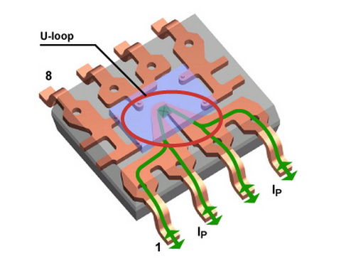
For small nominal currents up to ± 20 A, the Hall chip and main current path are packaged in standard size SOIC8 surface mount packaging, as shown in Figures 1 and 3. This provides a compact, slim solution that is compatible with large-scale automated circuit board assembly technology. The use of flip chip technology can optimize the magnetic coupling between the active surface of the Hall element and the magnetic field generated by the sensed current. Therefore, there is no need for a flux concentrator. The internal resistance of the copper path used for current detection is usually 1.5 m Ω to achieve low power consumption. The power terminal is also electrically isolated from the low-voltage signal I/O pin. Careful IC and packaging design can further improve the voltage isolation of devices,

Figure 1 shows the internal structure of the ACS package, showing a U-shaped primary copper conductor and a Hall IC installed on a single flip chip.

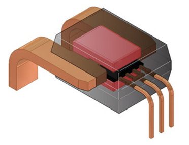
Figure 2 shows the internal structure of the CB package, showing the primary conductor (copper, left), flux concentrator (red), and linear sip Hall IC (black) and signal pins (copper, right).

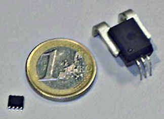
Figure 3: Photos of ± 20 A (LC package) and ± 200 A (CB package) current sensor ICs, displayed in coins for comparison.
Current up to 200 A
For higher currents, it is necessary to increase the cross-sectional area of the copper conductor to adapt to the current density within the materials provided in the CB package. Due to the magnetic coupling between thicker conductors and linear Hall elements, a flux concentrator must be used. The copper path, linear SIP Hall devices, and concentrators are assembled before encapsulation. Through carefully designed systems, the resistance of primary conductors is usually as low as 100? Ω, and a root mean square isolation voltage of 3 kV (60 Hz, lasting for 1 minute) can be achieved between the primary path and the signal side. Figure 2 shows the internal structure of this ± 200 A current sensor, and Figure 3 shows photos of the sensor and the ± 20 A packaging type.
|
Disclaimer: This article is transferred from other platforms and does not represent the views and positions of this site. If there is any infringement or objection, please contact us to delete it. thank you! |


