A Design Scheme for Extending the Battery Life of Wearable Devices through a Boost Voltage Stabilizer
Time:2023-05-19
Views:1022
Wearable devices have quickly become the latest "must-have" item in many people‘s daily life and work. Consumers use these devices to perform numerous tasks, most commonly monitoring health and managing busy schedules. In fact, the development momentum of wearable devices is so rapid that market research company ABI Research predicts a compound annual growth rate of 56.1% in the market, and its shipment volume will reach 487 million units in 2018. For the baby boomer generation entering old age, wearable devices come at the right time, as accurate medical monitoring can help address serious health issues. Due to the increasing expectations of users for device performance, system design engineers must develop smaller, more efficient, and more economical solutions to enable wearable devices to be worn on more people‘s wrists.
There are a wide variety of wearable devices, such as the Samsung Gear and Apple Watch, which can provide network connectivity, high-quality displays, and many features; In addition, there are wearable devices solely used for health monitoring, such as Fitbit Flex and Jawbone UP4, both of which have optimized data collection and fitness activity tracking functions. One of the most concerning issues for consumers in the context of the popularity of wearable devices is how long they can be used on a single charge. Battery life is a key consideration for consumers in deciding which wearable device to purchase.
This article introduces the system module design of typical wearable devices and analyzes how a boost buck regulator can improve power efficiency and extend battery life. Wearable device system design engineers will understand how a new voltage regulator uses adaptive current limiting pulse frequency modulation (PFM) and forced bypass mode to provide a smooth transition from voltage reduction to voltage increase, in order to prevent signal glitches in wearable device applications. Light load efficiency and fast transient response are crucial in these applications.
Wearable Device Architecture
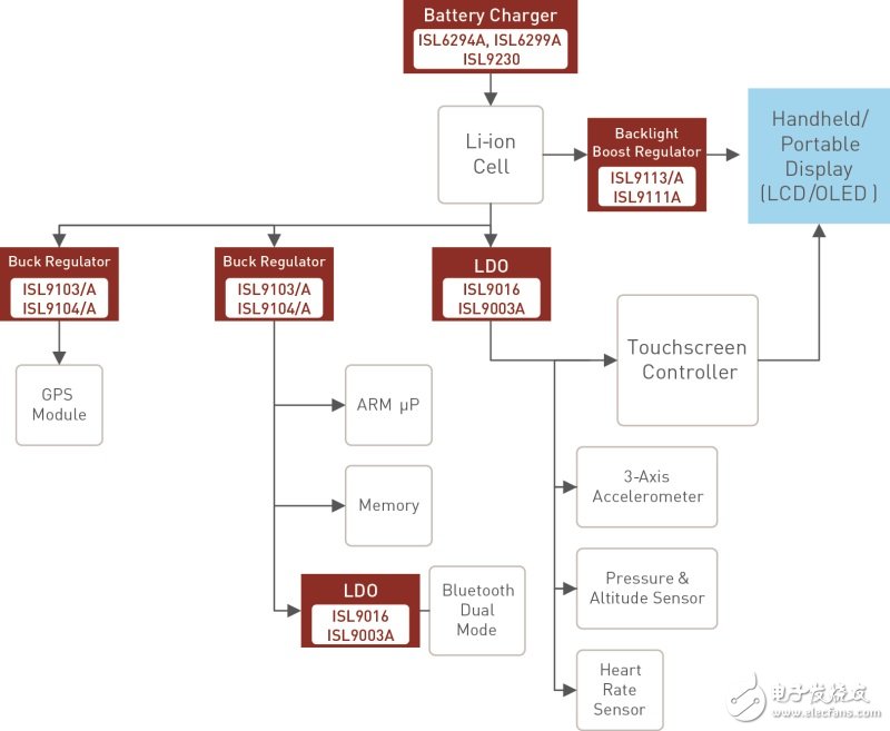
A typical wearable device architecture includes components such as microprocessors, memory, displays, sensors, communication ICs, and battery charging blocks. According to the specific system application, it is necessary to use at least 3 DC-DC converters and 3-5 LDO low voltage differential linear regulators. Figure 1 shows a typical power system for basic wearable devices.

Figure 1: Typical power supply solution system diagram for wearable devices
Battery charger:
Li ion Cell: Lithium ion battery
Backlight boost regulator
Handheld/portable display:
Buck regulator
GPS Module: GPS Module
Memory: Memory
Bluetooth Dual Mode: Bluetooth Dual Mode
Touchscreen controller: Touch screen controller
3-Axis accelerometer
Pressure&altitude sensor
Heart rate sensor
Firstly, we will discuss how boosting and lowering voltage regulators can add value to wearable systems. For applications that require an input voltage of approximately 3.3V~3.6V, a step-up and step-down regulator can efficiently use a wide range of new chemical batteries with a voltage range of 4.375V~2.5V. The boost buck voltage regulator is in pure boost mode when the battery voltage (Vbat) is 2.5V-3V, then in boost buck mode when Vin ≥ 3V and<3.9V, and finally in pure boost mode when Vbat=3.9V-4.5V.
Boost buck converter used as a pre regulator
Multiple applications such as WiFi and display modules are powered by a single LDO. If the power comes directly from the battery, these peripherals will generate significant power losses because the efficiency of LDO is equal to Vout divided by Vin. At higher loads, LDO has higher power loss and generates more heat. Using a boost buck converter as a pre regulator for LDO can help improve system efficiency. In addition, using this configuration, LDO always experiences constant Vin (boost buck output) power loss, which can avoid significant power loss caused by direct battery power supply. In addition, adding more wearable device features also requires faster processing speed, which drives the need for more efficient power management. When multiple applications are working simultaneously, short-term high current pulses can cause local node voltage to drop below the recommended input range and cause application shutdown. This situation is very unfavorable and can be avoided by using a boost buck converter as a pre regulator for these devices, such as liquid crystal displays (LCD) and applications powered by LDO.
Extend battery life
The ISL9120 boost buck regulator can provide excellent efficiency under both low load and high load conditions. As shown in Figure 2, its adaptive pulse frequency modulation (PFM) operating mode can help it achieve efficiency of up to 98% at higher loads and over 86% at lower load conditions. This ensures a reduction in power consumption and heat generation, thereby extending battery life and saving circuit board space by eliminating the need for external heat sink. To achieve efficiency optimization in the output current range, ISL9120 implements a multi-level current limitation scheme, divided into 32 levels from 350mA to 2A.
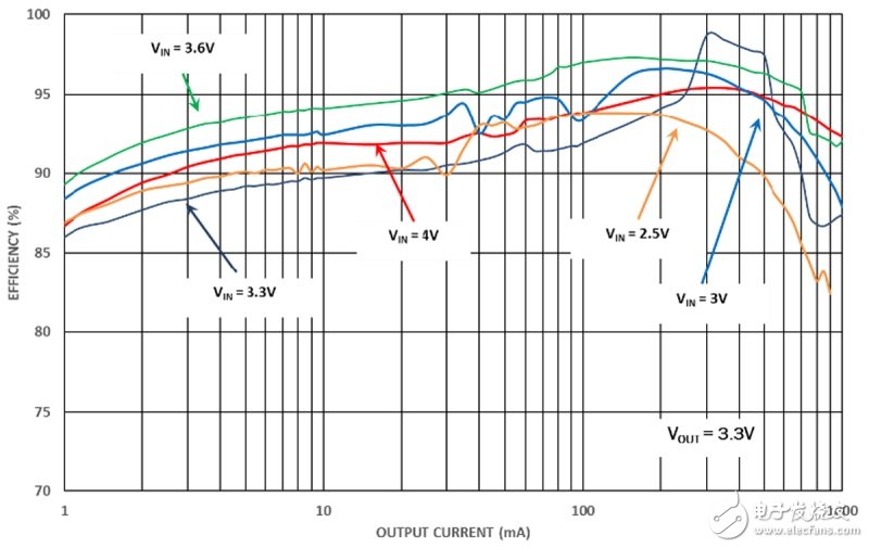

Figure 2: Efficiency Curve of ISL9120 Boost Step-down Stabilizer
As shown in Figure 3, the conversion from one level to another is determined by the number of pulses in a PFM pulse train. At a given peak current limit level, the number of pulses will increase as the output current increases. When the number of pulses reaches the upper limit threshold of the existing current limit, the current limit switches to the next higher level. Similarly, if the number of pulses reaches the lower threshold of the existing current limit, the device will transition to the next lower level of peak current limit. If the number of pulses reaches the upper limit threshold at the highest current limit, the current limit will no longer increase. ISL9120 also supports forced bypass mode, which eliminates the need for output regulation. The standby mode of its system has achieved less than 0.5 μ A‘s ultra-low static current consumption. For example, a step-up and step-down voltage regulator will use forced bypass mode when supplying power to the LDO and the LDO is in standby mode with output current close to zero. Under this condition, entering the bypass mode of the step-up/step-down regulator has little effect on LDO, but can save 41 µ A of static current consumption for the regulator.
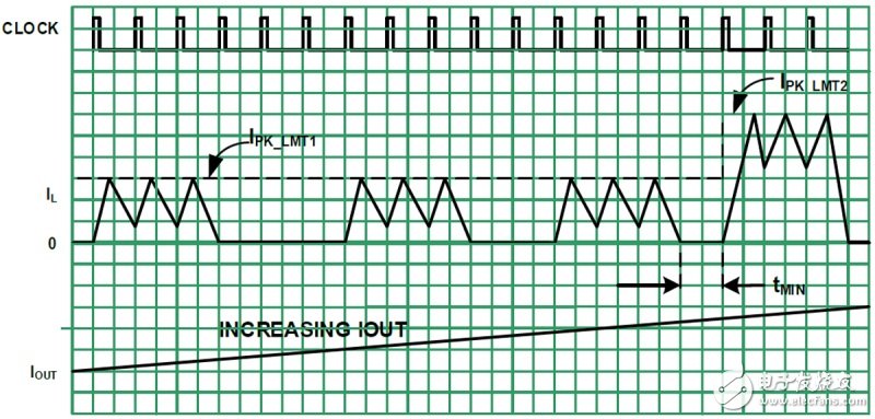

Figure 3: Adaptive current scheme provides a smooth transition from step-down to step-up
Increasing Iout: Increasing Iout
Examples of Boost/Depressurization Applications
Upon careful observation of Figure 1, it can be seen that wearable device applications using a step-up and step-down voltage regulator have advantages. For example, a heart rate monitor sensing system requires an input voltage of approximately 3.3V, and system design engineers typically recommend using 2-3 LEDs to accurately monitor heart rate, as this has less dependence on the wearing position of wearable devices and is suitable for a wider range of end users. But this configuration requires a significant amount of current consumption. The use of ISL9120 as a pre regulator is very suitable for this application, as the battery can directly power it, providing higher system efficiency (longer battery life), higher resistance to input disturbances, and extremely low output ripple. When the heart rate monitor is not working, ISL9120 can enter forced bypass mode, which only consumes 0.5 µ A of current until it is awakened.
The wearable LCD has a small size and typically uses a white LED as the backlight. As shown in Figure 1, the existing solution uses a 5V boost to power the LCD block. A wide range of small size (1-2 inches) LCDs can be powered by 3V~3.6V instead of 5V power supply. This makes the boost buck voltage regulator very attractive for achieving more efficient power supply design. Finally, wearable devices have a trend towards integrated WiFi, and such systems typically require a 3.3V power supply voltage and low input ripple. Due to the space limitations of wearable devices, a small and compact design is a fundamental requirement. Using ISL9120 as a pre regulator is very suitable for wearable device applications.
conclusion
Due to the smaller size and higher integration of wearable devices, faster processors are needed to manage more and more functions, making efficient power management particularly important. It has been proven that a new boost buck voltage regulator with adaptive current limiting PFM can meet these increasing requirements while extending battery life and enabling next-generation wearable devices to operate continuously for longer periods of time and at lower operating temperatures.
|
Disclaimer: This article is transferred from other platforms and does not represent the views and positions of this site. If there is any infringement or objection, please contact us to delete it. thank you! |


