Design Scheme and Operating Characteristics of LDO Linear Voltage Stabilizer
Time:2023-05-18
Views:1024
LDO (Low Voltage Differential) linear regulators have been widely used in portable electronic products due to their simple structure, low cost, low noise, and small size.
In portable electronic products, higher power efficiency means longer battery life, while linear regulator efficiency=output voltage × Output current/input voltage × Input current × 100%, therefore, the lower the input and output voltage difference, the lower the static current (difference between input current and output current), and the higher the working efficiency of the linear regulator.
The low voltage differential linear regulator designed in this article has an output voltage of 2.5V or adjustable output, which meets the minimum input output voltage difference of 0.4mV when the load is 1mA, 120mV when the load is 300mA, and the working range of power supply voltage is 2.5-6V
Circuit structure and working principle
The circuit structure of a low voltage differential linear regulator is shown in Figure 1. The circuit is composed of modules such as an adjustment tube, bandgap reference voltage, error amplifier, fast start, overcurrent limit, overheat protection, fault detection, and sampling resistor network, and has functions such as enabling and adjustable output. To meet the requirements of this design, the selection of the adjustment transistor as a load device for pressure difference needs to be carefully considered: firstly, compare the transistor and MOS transistor. As the transistor is a flow controlled device, while the MOS transistor is a voltage controlled device, the static current of the MOS transistor structure is relatively lower. Secondly, NMOS transistors require a driving signal higher than the output voltage when working, while PMOS transistors do not have this requirement, especially when generating a high driving voltage at low input voltage becomes more difficult. Therefore, this article uses PMOS transistor as the adjustment transistor.
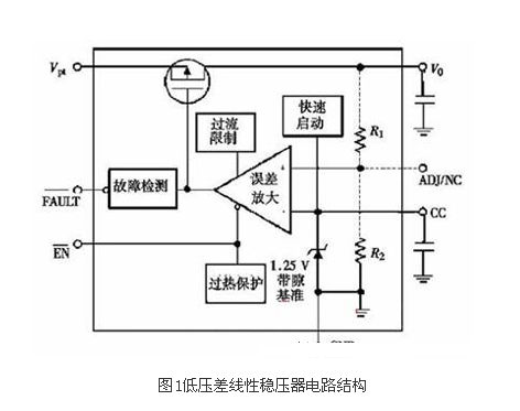
Figure 1 Circuit structure of low voltage differential linear regulator
The working principle of the circuit is that during the process of powering on the circuit, there is a 500 μ The current source of A charges the bypass capacitor C at the CC end to enable the circuit to power on and start as soon as possible. The same phase end of the error amplifier samples the output voltage V0 through sampling resistors R1 and R2, and then compares it with Vref to output an amplification signal. Control and adjust the gate voltage of the PMOS transistor to maintain stable output voltage V0, that is:

When overcurrent or overheating occurs during the operation of the circuit, the overcurrent limit and overheating protection circuit will respond quickly, and the conduction state of the adjustment tube will be weakened or turned off to protect the circuit from damage. At the same time, the fault detection circuit will generate a low-level signal. Enable the termination of high voltage circuits to operate normally; When the enabling end is at low level, the reference circuit and the adjustment PMOS transistor are turned off, and the circuit is in a waiting state.
Key Characteristic Analysis and Design Considerations
1. Leakage voltage (VDO) and quiescent current (Iq)
The leakage voltage is defined as the minimum input output voltage difference that maintains the normal operation of the voltage regulator, and it is an important factor reflecting the adjustment ability of the regulator. For circuits using PMOS transistors as adjustment transistors, the leakage voltage is determined by the conduction resistance (Ron) and load current (Io), i.e. VDO=Io × The static current of Ron‘s low voltage differential linear regulator is the difference between the input current and the output current, i.e. Iq=Ii Io. The static current is composed of the bias current and the gate driving current of the regulating transistor. For PMOS tuning transistors, the gate is driven by voltage and generates almost no power consumption. When the voltage regulator carries a small load or no load, the leakage voltage is extremely low, and the static current is equal to the total bias current of the voltage regulator during operation. During design, attention should be paid to minimizing the conduction resistance and leakage current of the PMOS adjustment transistor, so that each module circuit can operate normally under low current conditions.
2. Power consumption (Pw) and efficiency( η)
The power consumption of a low voltage differential linear regulator is the difference between input energy and output energy, which is:
PW = VI II - VO IO = ( VI - VO) IO + VI Iq
In the above equation, the former is the power consumption generated by the adjustment tube, and the latter is the static current power consumption. The efficiency of the voltage regulator can be expressed as follows:
η= IO VO / ( IO + Iq ) VI × 100 %
The expression of power consumption and efficiency fully demonstrates that for low voltage differential linear regulators, low leakage voltage and low static current mean low power consumption and high efficiency.
3. Load adjustment capability and voltage adjustment capability
Load adjustment capability refers to the ability to maintain a certain value of output voltage when the output current changes, defined as: Δ VO / Δ IO, which represents the ability of the voltage regulator to maintain the output at the nominal value due to load changes, the smaller the value, the better. Voltage regulation ability refers to the ability to maintain a certain value of output voltage when the input voltage changes, defined as: Δ VO / Δ VI. It characterizes the ability of the voltage regulator to maintain the output at the nominal value while the input voltage changes, and the smaller the value, the better. The load adjustment ability and voltage adjustment ability of the circuit structure in Figure 1 are:
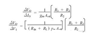
Where gm is the transconductance of the adjustment tube; Aod is the open-loop differential mode gain of the error amplifier; Rds is the equivalent resistance between the source and drain of the adjustment tube; RL is the load resistance; R1 and R2 are sampling resistors. As can be seen from the above equation, decrease Δ VO÷ Δ IO and Δ VO÷ Δ The key to VI is to maximize gm and Aod as much as possible
4. Transient response
Transient response is the dynamic characteristic of voltage regulator, which refers to the transient pulse phenomenon of output voltage caused by the step change of load current and the time when the output voltage recovers to stability. It is related to the output capacitance COUT, the equivalent series resistance RESR of output capacitance, and the bypass capacitance Cb. The maximum transient voltage pulse value Δ VTR (MAX) is:
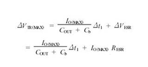
Among them, IO (MAX) refers to the maximum load current that undergoes a step change; Δ T1 is the response time of the regulator closed-loop, which is related to the regulator closed-loop bandwidth (0dB frequency point). When designing applications, it is necessary to consider reducing the transient voltage pulse of the voltage regulator, that is, increasing the bandwidth of the voltage regulator, increasing the output and bypass capacitance, and reducing its equivalent resistance.
5. Output accuracy
The output accuracy of a voltage regulator is reflected by the combined effect of various factors on the output terminal, mainly including output changes caused by changes in input voltage Δ Output changes caused by VLR and load changes Δ Output changes caused by VLDR and reference drift Δ Output changes caused by Vref and error amplifier misalignment Δ Output changes caused by Vamp and sampling resistance drift Δ Vres and output changes caused by changes in operating temperature Δ VTC, output accuracy ACC is given by the following equation:

among Δ Vref、 Δ Vamp and Δ Vres has a significant impact on ACC, so the topology structure of the reference voltage source, error amplifier, and sampling resistor network needs to be carefully considered during design.
Circuit design and simulation results
1. Design of Bandgap Reference Voltage Source
The reference voltage source is the core module of a linear voltage regulator and the most important factor affecting the accuracy of the regulator. The operating principle of the bandgap voltage reference is to use the negative temperature coefficient of the transistor‘s VBE and the Δ The positive temperature coefficient characteristic of VBE is multiplied by an appropriate coefficient to compensate each other, thus obtaining the output voltage of low-temperature drift.
The circuit implementation is shown in Figure 2, including:

Where n is the emission area ratio of Q1 and Q2. The HspICE simulation results indicate that when the power supply voltage changes in the range of 2.5~6V, VREF=1.254V at room temperature, and the temperature change range is between -30~120 ℃, the temperature drift coefficient is less than 10 × 10-6/℃。
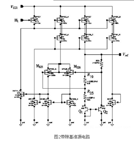
Figure 2 Bandgap Reference Circuit
2. Design of Error Amplifiers
The error amplifier compares and amplifies the difference signal between the output feedback sampling voltage and the reference voltage. After output, it controls the conduction state of the adjustment tube to maintain Vout stability. Its gain, bandwidth, and input offset voltage have a significant impact on the output accuracy, load and voltage adjustment ability, transient response, and other characteristics of the regulator. The circuit implementation is shown in Figure 3. By simulating with HspICE, the input offset voltage of the error amplifier is 0.05 when VCC1 is 4.2V μ V. The DC gain is 110dB and the bandwidth reaches 10MHz
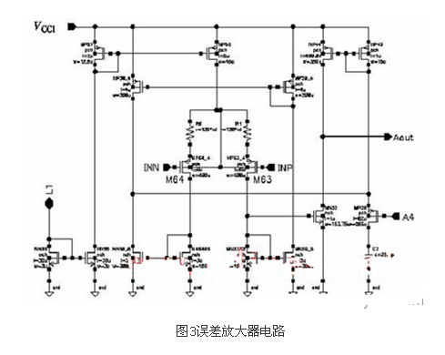
Figure 3 Error amplifier circuit
3. Design of overcurrent limiting module
The design concept of the overcurrent limiting circuit is to control the gate voltage of the regulating transistor by sampling the gate source voltage of the regulating transistor, thereby achieving the goal of limiting the output current. The circuit implementation is shown in Figure 4.
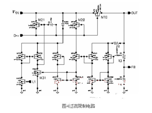
Figure 4 Overcurrent limiting circuit
When the load current increases from small to large, VDrv decreases and the ID of the adjustment tube MTG increases. By sampling the gate source voltage of the adjustment tube MTG through M20, the gate voltage of M31 increases, and the gate voltage of M21 decreases accordingly, thus achieving VDrv adjustment. Through Hspice simulation, it was found that when the load current exceeds 330mA, M21 will start to conduct, thereby increasing VDrv and weakening the MTG conduction degree of the adjustment tube, providing current limiting protection.
3.4 Design of overheat protection module
The design concept of the overheat protection circuit is to use temperature sensitive components to detect changes in the temperature inside the chip. When the temperature exceeds the set value, the protection circuit acts and the adjustment tube is turned off to prevent damage. The circuit implementation is shown in Figure 5.
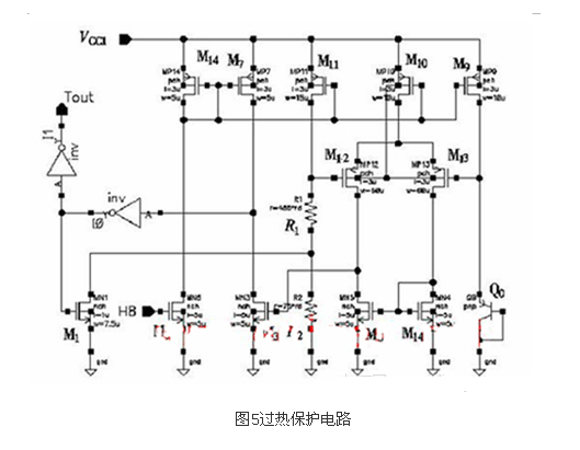
Figure 5 Overheat Protection Circuit
The VBE of the transistor has the characteristic of negative temperature coefficient. Q0 is used as a temperature measuring element. M12, M13, M10, M5, and M4 form a comparator, and M11, R1, and R2 form a voltage divider circuit. When the temperature is lower than the set value, design VGM12 VGM13, reverse the comparator, turn VGM3 to a high level, and output TOUT to a low level, thus achieving the shutdown adjustment tube. The temperature protection setting of this circuit is 160 ℃, and the simulation results of Hspice are shown in Figure 6 × Represents the output voltage VOUT, ⊙ represents VGM12, Δ Represents VGM13, with a load current of 300mA
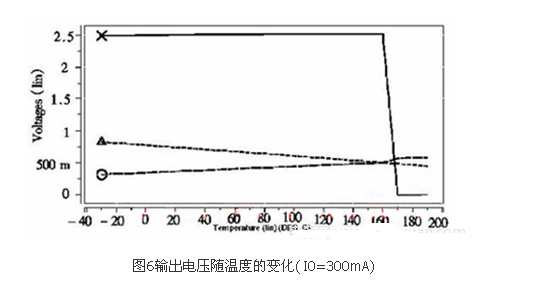
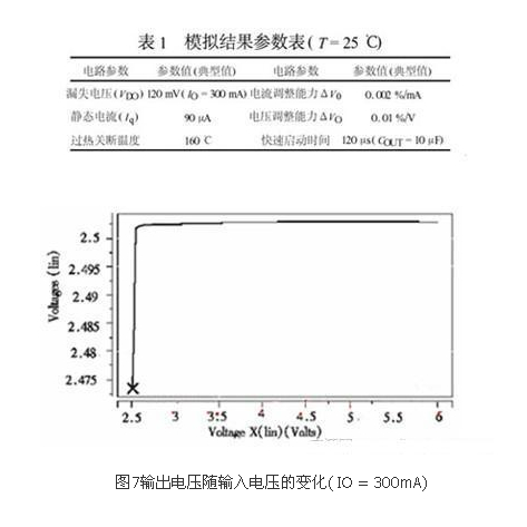

Figure 6: Change of output voltage with temperature (I0=300mA)
3.5 Overall Circuit Simulation Results
This circuit adopts Hyundai Corporation of Korea 0.6 μ The M process model was simulated and optimized using Hspice for the overall circuit and key modules. The simulation results under typical working conditions are shown in Table 1, and the variation of output voltage with input voltage and temperature is shown in Figures 6 and 7. The simulation results fully validate the correctness of the design.

Figure 7: Change of output voltage with input voltage (IO=300mA)
4 Summary
This plan analyzes and discusses the design scheme and operating characteristics of a low voltage differential linear regulator, and provides circuit design diagrams of key modules. The simulation results of HSPICE verify that the circuit has good characteristics. The circuit is implemented using standard CMOS technology, which has high practical value.
|
Disclaimer: This article is transferred from other platforms and does not represent the views and positions of this site. If there is any infringement or objection, please contact us to delete it. thank you! |


