Design of a Novel Class D Audio Power Amplifier Driver Circuit
Time:2023-03-18
Views:1140
Due to the high efficiency and relatively small size of the integrated Class D audio power amplifier, and in most cases, no or only a small area of heat sink is required, greatly reducing the overall size, making it the preferred choice in audio electronics products. However, when using the same layout area in the design of Class D power amplifiers, the on-resistance of pMOS transistors is much greater than that of nMOS transistors. In order to reduce the layout area and the H-bridge on-resistance of the output stage of Class D power amplifiers, nMOS transistors are used for the H-bridge. In order to equalize the overdrive voltage of the LDNMOS transistors at the high and low ends of the H-bridge, it is necessary to add an additional high-level power supply to drive the high end of the H-bridge. Therefore, it is necessary to use a capacitor bootstrap circuit based on a charge pump to generate a high-level. This not only improves the driving efficiency, but also reduces the need for multiple external power supplies, cleverly realizing the driving of the H-bridge of the Class D power amplifier.

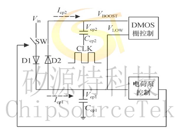
The following diagram shows the schematic diagram of a Class D power amplifier driver circuit. Vin is the power supply, D1 and D2 are charging diodes, Ccp1 is a storage charge capacitor, and Ccp2 is a bootstrap capacitor (connected to Vboost at one end and clk signal at the other end). Icp1 charges the capacitor Ccp1 and generates a voltage Vcp1 through charge pump control, thereby Vcp1 serves as the driving level for driving the H-bridge low-end LDNMOS transistor; Icp2 is used to charge the capacitor Ccp2, and the voltage Vcp2 is generated by the bootstrap of the capacitor Ccp2, so that Vcp2 serves as the driving level for driving the H-bridge high-end LDNMOS transistor. The charge pump control module mainly controls the charging and discharging process of the loop capacitor Ccp1 and the generation of the bootstrap voltage Vcp2. The following discussion focuses on the generation of high and low levels in Class D power amplifier drive circuits, the control loop mechanism of the charge pump, and the working principle of the entire drive circuit.

Class D power amplifier drive circuit topology diagram
|
Disclaimer: This article is transferred from other platforms and does not represent the views and positions of this site. If there is any infringement or objection, please contact us to delete it. thank you! |


