Design and Research of Current Limiting Protection Circuit Based on PWM
Time:2022-11-06
Views:1624
Abstract: A very important content in the design of switching power supply is the design of overload protection function, especially in the space field. Because of its special requirements of high reliability, high risk and non maintainability, the space DC-DC converter should have reliable overload protection function.

1 Introduction
The function of overload protection is to effectively protect the DC-DC converter from being damaged due to overheating when the load is overloaded, that is, to control the overload current (input current) of the power MOSFET. Due to different electrical loads, the requirements for overload protection functions are also different. If the satellite control system requires that the DC-DC converter cannot be powered off after overload, current limiting protection is adopted; The payload system requires that the DC-DC converter can be powered off after overload, so current cutoff protection is adopted. This paper presents a design method of current limiting protection circuit based on PWM, and the design verification.
2. Over current protection of current loop control mode
The current mode control is a double loop control system, which is composed of a current loop (inner loop) fed back by the peak current signal of the switching device and a voltage loop (outer loop) fed back by the output voltage signal. The power conversion part is the current source controlled by the current loop, and the voltage outer loop controls the current loop of the power stage. The inner current loop is responsible for the dynamic change of the output inductance, while the outer voltage loop only needs to control the output capacitance.
There are many current mode PWM control modes, such as UC1842 (3, 4, 5) series, UC1846, UC1825 (voltage mode and current mode), etc. All of them have designed overcurrent protection functions based on current loop.
Taking UC1842 as an example, its working principle is that the power switch starts to conduct from the oscillator and terminates when the peak inductance current reaches the threshold level established by the output of the error amplifier, so that the error signal fed back on a weekly basis controls the peak inductance current. That is, the current sampling signal is compared with the output level of the error amplifier cycle by cycle, and the drive pulse is generated to control the turn-on time of the power switch, so as to achieve closed-loop output. In the over-current state, due to the large slope of the peak inductance current, the drive pulse generated by the cycle by cycle comparison is very narrow, which greatly limits the conduction time of the power switch, realizes current limiting protection, and is a peak current control mode. The peak inductance current is controlled by the output voltage of the error amplifier, as shown in Formula (1):

Where: VE is the output voltage of the error amplifier; RS current detection resistance.

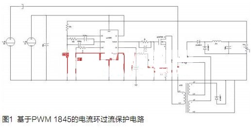
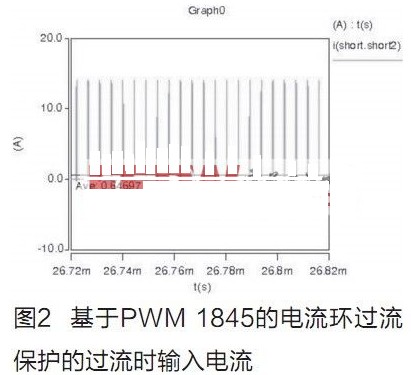
However, according to many years of engineering practice, the over-current protection relying only on the current loop control mode cannot effectively limit the input current, and the circuit simulation and test results are relatively consistent. The following is the simulation results of the current loop over-current protection based on PWM 1845. The simulation circuit is shown in Figure 1 and the result is shown in Figure 2. It can be seen that the average input current after overcurrent is 0.65A

The overcurrent protection of the reverse input terminal of PWM error amplifier is controlled by current sampling signal
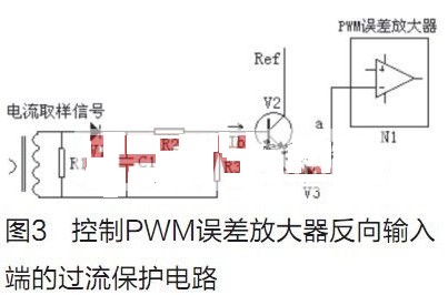
In order to effectively limit the input current after over-current, an over-current protection circuit using current sampling signal to control the reverse input end of PWM error amplifier is designed, as shown in Figure 3.

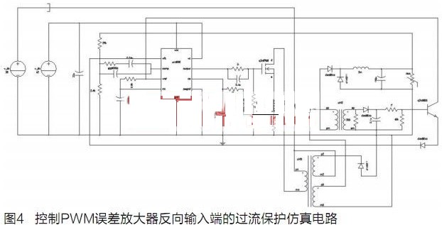
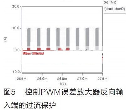
The basic working principle of the circuit is as follows: the triode V2 in Figure 3 is connected to the emitter follower form, and the current signal at the output end collected by the current transformer is used as the control signal to control V2. During normal output, the voltage of the current sampling signal is very low, making the output voltage of the emitter follower lower than the set level of the reverse input end (feedback end) of the error amplifier. The over-current protection circuit shown in Figure 3 does not affect the normal output characteristics of the DC-DC converter. When the output over-current occurs, the current sampling signal voltage increases, making the output voltage of the transmitter follower higher than the set level of the reverse input terminal of the error amplifier. The output voltage Ve of the error amplifier decreases, and the PWM drive signal narrows, making the output voltage decrease, and the input current finally stabilizes at a certain value. The simulation circuit is shown in Figure 4 and the results are shown in Figure 5. It can be seen that the average input current after overcurrent is 0.157A

4. Over current protection of PWM error amplifier output terminal controlled by current sampling signal

It can be seen from the above circuit that compared with the over-current protection using PWM current loop directly, the input current is significantly reduced, but there is still 0.157A current at the source end, mainly because the control mode is average current control mode. The over-current control signal is to sample and rectify the output current into a DC signal, and form a driving pulse through the input end of the error amplifier. Therefore, when the overload occurs, the over-current control signal formed after several cycles of accumulation is input to the reverse input terminal of the error amplifier, making the error amplifier output low. At this time, there is no drive pulse output, and the power output decreases; After several cycles, as the power output decreases, the over-current control signal also decreases. At this time, the drive pulse output is generated to increase the power output. This cycle makes the power supply oscillate intermittently. As can be seen from Figure 5, the input current is also an intermittent oscillation waveform.
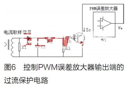
In order to further optimize the overcurrent protection mode, the overcurrent protection circuit shown in Figure 3 is improved as follows: connect the collector of control tube V2 to the output end of the error amplifier, and the radiation stage is grounded. As shown in Figure 6.

When the DC-DC converter works in the normal closed loop state, the PWM error amplifier works in the linear amplification area, and its output level depends on the input error signal level and the amplifier gain. The triode V2 in Figure 6 operates in the cut-off zone, and the over-current protection circuit shown in Figure 6 does not affect the normal output characteristics of the normal DC-DC converter.
5 Conclusion
The over-current protection circuit based on PWM designed in this paper is a general over-current protection circuit of DC-DC converter, which has high reliability and can effectively protect DC-DC converter from damage due to overheating when it is overloaded.
|
Disclaimer: This article is transferred from other platforms and does not represent the views and positions of this site. If there is any infringement or objection, please contact us to delete it. thank you! |


