11 Golden Rules Easily Handle DCDC Power Conversion Circuit Design
Time:2024-03-21
Views:233
11 Golden Laws for Designing DC-DC Power Conversion Circuits.
Engineers who specialize in embedded systems often excel in microcontroller, ARM, DSP, and FPGA. However, once designing a system and supplying power to the power system, although carefully designed programs can still run, it may sometimes be inefficient for beginners, and there may also be problems caused by insufficient or excessive power supply current. This article provides 11 rules to easily solve the design of DC-DC power conversion circuits.
01 Understand what‘s going on with the DC-DC power supply
The DC-DC power supply circuit, also known as the DC-DC conversion circuit, mainly functions to convert input and output voltage. Generally, we refer to the voltage conversion process where the input power supply voltage is within 72V as DC-DC conversion. The common power supplies are mainly divided into vehicle and communication series and general industrial and consumer series. The former uses voltages such as 48V, 36V, 24V, etc., while the latter uses power supply voltages generally below 24V. The rules vary in different application fields, such as 12V, 5V, and 3.3V commonly used in PCs, 5V and 15V commonly used in analog circuit power supplies, and 3.3V commonly used in digital circuits. Nowadays, FPGA and DSP also use voltages below 2V, such as 1.8V, 1.5V, 1.2V, etc. In communication systems, also known as secondary power supply, it is a DC input voltage provided by a primary power supply or DC battery pack, and after DC-DC conversion, it obtains one or several DC voltages at the output end.
02 Classification of DC-DC conversion circuits that need to be known
DC-DC conversion circuits are mainly divided into the following three categories:
1. Voltage regulator circuit. ② Linear (analog) voltage stabilizing circuit. ③ Switch type voltage stabilizing circuit
03 The simplest voltage regulator circuit design scheme
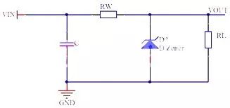
The structure of the voltage regulator circuit is simple, but it has poor load capacity and low output power. Generally, it only provides reference voltage for the chip and is not used as a power source. The commonly used type is the parallel voltage stabilizing circuit, and its circuit diagram is shown in Figure (1):

When selecting a voltage regulator, it can generally be estimated using the following formula: (1) Uz=Vout; (2) Izmax=(1.5-3) ILmax (3) Vin=(2-3) Vout This circuit has a simple structure and can suppress input voltage disturbances. However, due to the limitation of the maximum operating current of the voltage regulator and the inability to adjust the output voltage arbitrarily, it is suitable for situations where the output voltage does not need to be adjusted, the load current is small, and the requirements are not high. This circuit is commonly used for supplying power to chips that do not require high supply voltage.
04 Reference voltage source chip voltage stabilizing circuit
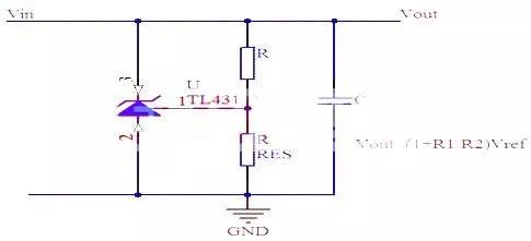
Another form of voltage stabilizing circuit, some chips have high requirements for power supply voltage, such as the reference voltage of AD DA chips. In this case, commonly used voltage reference chips such as TL431, MC1403, REF02, etc. TL431 is the most commonly used reference source chip and a three terminal adjustable shunt reference voltage source with good thermal stability performance. Its output voltage can be arbitrarily set to any value within the range of Vref (2.5V) to 36V using two resistors. The most commonly used circuit application is shown in the following diagram, where Vo=(1+R1/R2) Vref. Choosing different values of R1 and R2 can yield any voltage output in the range of 2.5V to 36V. Specifically, when R1=R2, Vo=5V.

The other reference voltage source chip circuits are similar.
05 Circuit Understanding of 05 Series Stabilized Power Supply
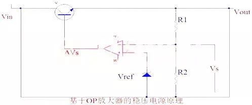
Series voltage regulator circuit belongs to a type of DC voltage regulator power supply. It is actually a commonly used DC power supply method before the emergence of three terminal voltage regulators. Before the emergence of three terminal voltage regulators, series voltage regulators usually had an OP amplifier and a voltage regulator diode to form an error detection circuit, as shown in the following figure. In this circuit, the reverse input terminal of the OP amplifier is connected to the detection signal of the output voltage.
The forward input terminal is connected to the reference voltage Vref, where Vs=Vout * R2/(R1+R2). Due to the amplification of the signal Δ Vs is a negative value that controls the decrease in the base voltage of the transistor, resulting in a decrease in output voltage. Under normal circumstances, there must be Vref=Vs=Vout * R2/(R1+R2). Adjusting the ratio of R1 to R2 can set the desired output voltage value.
The diagram only shows the basic principle of a three terminal voltage regulator. In fact, the load size can be changed from a transistor to a Darlington transistor, and so on. Improper handling of this series type voltage regulator circuit as a DC voltage regulator can easily cause oscillation. There are currently no engineers with certain simulation skills, and this method is generally not used now. Instead, an integrated three terminal voltage regulator circuit is directly used for the use of DC-DC conversion circuits.

06 Common design schemes for linear (analog) integrated voltage stabilizing circuits
The design scheme of linear voltage regulator circuit mainly focuses on three terminal integrated voltage regulators. There are two main types of three terminal voltage regulators:
One type of output voltage is fixed, called a fixed output three terminal voltage regulator. The universal products of three terminal voltage regulators include 78 series (positive power supply) and 79 series (negative power supply). The output voltage is represented by the last two digits in the specific model, and there are grades such as 5V, 6V, 8V, 9V, 12V, 15V, 18V, 24V, etc. The output current is distinguished by adding a letter after 78 (or 79). L represents 0.1A, M represents 0.5A, and no letter represents 1.5A. As shown in the 78L05 table, calculate 5V 0.1A.
Another type of output voltage is an adjustable linear regulator circuit, called an adjustable output three terminal regulator. This type of chip is represented by the LM317 (positive output) and LM337 (negative output) series. Its maximum input output limit difference is 40V, the output voltage is continuously adjustable from 1.2V-35V (-1.2V-35V), the output current is 0.5-1.5A, the voltage between the output end and the adjustment end is 1.25V, and the static current at the adjustment end is 50uA.
The basic principle is the same, all of which use series voltage stabilizing circuits. In linear integrated voltage regulators, due to the fact that the three terminal voltage regulator only has three lead out terminals, it has the advantages of fewer external components, convenient use, stable performance, and low price, and is widely used.
07.Design scheme of 07 DCDC conversion switch type voltage stabilizing circuit
The above mentioned DCDC conversion circuits all belong to the series feedback voltage stabilizing circuit. In this working mode, the regulator in the integrated voltage stabilizer works in the linear amplification state, so when the load current is large, the loss is relatively large, that is, the conversion efficiency is not high. Therefore, the power of power circuits using integrated voltage regulators is not very high, usually only 2-3W, and this design scheme is only suitable for low-power power circuits.
The DC-DC conversion circuit designed with a switching power supply chip has high conversion efficiency and is suitable for high-power power supply circuits. At present, it has been widely used, commonly divided into non isolated switching power supplies and isolated switching power supply circuits.
The design scheme of DCDC conversion switch type voltage stabilizing circuit adopts a switching power supply chip design, which has high conversion efficiency and is suitable for high-power power supply circuits. At present, it has been widely used, commonly divided into non isolated switching power supplies and isolated switching power supply circuits. Of course, the basic topologies of switch mode power supplies include step-down, step-up, step-down, flyback, forward, bridge variations, and so on.
08.Design scheme of 08 non isolated DCDC switch conversion integrated circuit chip circuit
The use of DCDC switch conversion integrated circuit chips is very similar to LM317 in Article 6. Here, L4960 is used as an example. Generally, a 50Hz power transformer is first used for AC-AC conversion, reducing~220V to the input voltage range of the switch power integrated conversion chip, such as 1.2-34V, and then L4960 is used for DC-DC conversion. At this time, the range of output voltage can be adjusted to 5V, increased to 40V, and the maximum output current can reach 2.5A (high-power switching tubes can also be connected for current expansion). It is equipped with complete protection functions such as overcurrent protection and overheating protection.
Although the usage method of L4960 is similar to LM317, the efficiency of L4960 in switch mode power supply is not the same as that of LM317 in linear mode power supply. L4960 can output a maximum power of 100W (Pmax=40V * 2.5A=100W), but it only consumes a maximum of 7W, so the heat sink is small and easy to manufacture.
Similar to L4960, there is L296, which has the same basic parameters as L4960, except that the maximum output current can reach 4A and it has more protection functions, and the packaging form is also different. There are many such chips, such as LM2576 series, TPS54350, LTC3770, and so on. Generally, when using these chips, manufacturers provide detailed instructions and typical circuits for reference.
09.Design scheme of 09 isolated DCDC switching power supply module circuit
09.Design scheme of 09 isolated DCDC switching power supply module circuit
The commonly used isolated DC-DC conversion can be divided into three categories:
1. Flyback transformation; 2. Forward transformation; 3. Bridge transformation
The commonly used single ended flyback DC-DC conversion circuit has many types of isolated control chips. The typical representative of control chips is the commonly used UC3842 series. This is a high-performance fixed frequency current controller mainly used for isolating AC/DC and DC-DC conversion circuits. The main application principle is that the circuit consists of four parts: the main circuit, control circuit, starting circuit, and feedback circuit.
The main circuit adopts a single ended flyback topology, which is composed of a voltage rise and fall chopper circuit evolved with an isolation transformer. This circuit has the advantages of simple structure, high efficiency, and wide input voltage range. The control circuit is the core of the entire switching power supply, and the quality of control directly determines the overall performance of the power supply. This circuit adopts peak current type dual loop control, which adds peak current feedback control in the voltage closed-loop control system.
Choosing the appropriate transformer and MOSFET for this type of scheme can increase the power output significantly. Compared with the previous design schemes, the circuit structure is complex, and it is difficult to determine component parameters, resulting in higher development costs. Therefore, when this scheme is needed, priority can be given to choosing the relatively inexpensive DC-DC isolation module on the market.
010. DCDC Switch Integrated Power Module Solution
Many microprocessors and digital signal processors (DSPs) require a kernel power supply and an input/output (I/O) power supply, which must be sorted during startup. Designers must consider the relative voltage and timing of the core and I/O voltage source during power on and off operations to comply with the manufacturer‘s specified performance specifications.
If there is no correct power sorting, there may be blocking or excessive current consumption, which can cause damage to the I/O ports of supporting devices such as microprocessors, memory, programmable logic devices (PLDs), field programmable gate arrays (FPGAs), or data converters. To ensure that the kernel voltage is correctly biased before driving the I/O load, it is necessary to track the kernel power supply and I/O power supply.
There are now specialized power module companies that tailor some specialized switch mode power supply modules, mainly for DC-DC power modules with small size, high power density, high conversion efficiency, low heat generation, long mean time between failures, good reliability, lower cost, and higher performance, in addition to conventional electrical performance indicators.
These modules combine most or all of the components required to implement plug and play solutions, and can replace up to 40 different components. This simplifies integration and accelerates design, while reducing the board space occupied by power management.
The most traditional and common non isolated DC-DC power modules are still single in line (SiP) packages. These open framework solutions have indeed made progress in reducing design complexity. However, the simplest approach is to use standard packaged components on printed circuit boards.
011.Precautions for selecting the 011 DCDC power conversion scheme
This golden rule is also a summary of this article, which is very important. This article mainly introduces several commonly used design methods and schemes for three circuit modes of DCDC power conversion: voltage regulator, linear (analog) voltage regulator, and DCDC switch type voltage regulator.
① It should be noted that the voltage regulator circuit cannot be used as a power source and can only be used for chip power supply without power requirements;
② The linear voltage regulator circuit has a simple circuit structure, but due to low conversion efficiency, it can only be used in low-power voltage regulators;
③ The switch type voltage regulator circuit has high conversion efficiency and can be applied in high-power situations, but its limitation is that the circuit structure is relatively complex (especially in high-power circuits), which is not conducive to miniaturization. Therefore, in the design process, suitable design schemes can be selected according to actual needs.
|
Disclaimer: This article is transferred from other platforms and does not represent the views and positions of this site. If there is any infringement or objection, please contact us to delete it. thank you! |


