ESD suppression criteria in PCB design
Time:2024-03-10
Views:255
PCB design can reduce the unnecessary costs of fault detection and rework. In PCB design, due to the use of transient voltage suppressor (TVS) diodes to suppress direct charge injection caused by ESD discharge, it is more important to overcome the electromagnetic interference (EMI) electromagnetic field effect caused by discharge current in PCB design. This article will provide PCB design guidelines that can optimize ESD protection.
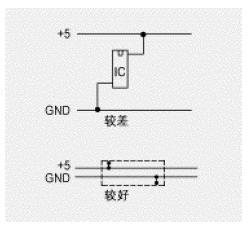
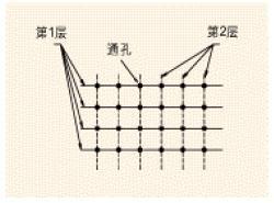 Grid connection can serve as a power source and grounding layer. Use via holes to connect the printed wires of each layer, and the spacing between via holes in each direction should be within 6 centimeters. In addition, when wiring, placing the power and ground printed wires as close as possible can also reduce the loop area, as shown in Figure 3.
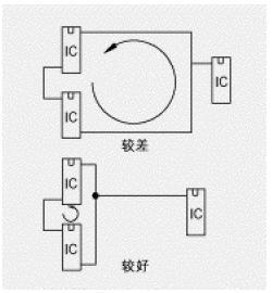
 Another method to reduce the loop area and induced current is to reduce the parallel paths between interconnect devices, as shown in Figure 4.
 When it is necessary to use a signal connection line longer than 30 centimeters, a protective line can be used, as shown in Figure 5.
 A better approach is to place strata near the signal line. The signal line should be within 13 millimeters of the protective wire or grounding wire layer. As shown in Figure 6, cross the long signal line (>30 cm) or power line of each sensitive component with its grounding wire. Cross connections must be arranged with regular intervals from top to bottom or from left to right.
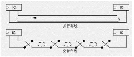
Circuit loop:

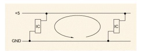
Current enters the circuit loops through induction, which are closed and have varying magnetic flux. The amplitude of the current is proportional to the area of the ring. A larger loop contains a greater amount of magnetic flux, which induces a stronger current in the circuit. Therefore, it is necessary to reduce the loop area. The most common loop, as shown in Figure 1, is formed by the power supply and ground wire. Under possible conditions, multi-layer PCB designs with power and ground planes can be used. The multi-layer circuit board not only minimizes the loop area between the power supply and ground, but also reduces the high-frequency EMI electromagnetic field generated by ESD pulses. If multi-layer circuit boards cannot be used, the wires used for power and grounding must be connected in a grid shape as shown in Figure 2.


Circuit connection length
Long signal lines can also serve as antennas for receiving ESD pulse energy, and using shorter signal lines as much as possible can reduce the efficiency of signal lines as antennas for receiving ESD electromagnetic fields. Try to place interconnected devices in adjacent positions to reduce the length of interconnected printed wires.
Ground charge injection
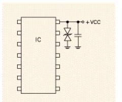
The direct discharge of ESD to the ground layer may damage sensitive circuits. Along with using TVS diodes, one or more high-frequency bypass capacitors should also be used, which are placed between the power supply and ground of vulnerable components. The bypass capacitor reduces charge injection and maintains the voltage difference between the power and ground ports. TVS divides the induced current and maintains the potential difference of the TVS clamp voltage. TVS and capacitors should be placed as close as possible to the protected IC (see Figure 7), ensuring that the TVS to ground path and capacitor pin length are the shortest to reduce parasitic inductance effects.

The connector must be installed on the copper platinum layer of the PCB. In an ideal situation, the copper platinum layer must be isolated from the grounding layer of the PCB and connected to the solder pad through a short wire.
Other guidelines for PCB design
1. Avoid arranging important signal lines at the edges of the PCB, such as clocks and reset signals;
2. Set unused parts on the PCB as grounding points;
3. The distance between the casing ground wire and the signal wire should be at least 4 millimeters;
4. Keep the aspect ratio of the casing ground wire less than 5:1 to reduce inductance effects;
5. Use TVS diodes to protect all external connections;
Parasitic inductance in protective circuits
The parasitic inductance in the TVS diode path can cause serious voltage overshoot when an ESD event occurs. Despite the use of TVS diodes, due to the induced voltage VL=L × di/dt at both ends of the inductive load, excessive overshoot voltage may still exceed the damage voltage threshold of the protected IC.
The total voltage borne by the protective circuit is the sum of the clamping voltage of the TVS diode and the voltage generated by the parasitic inductance, VT=VC+VL. An ESD transient induced current can reach its peak in less than 1ns (according to IEC 61000-4-2 standard), assuming a lead inductance of 20nH per inch, a line length of one quarter inch, and an overshoot voltage of 50V/10A pulses. The empirical design criterion is to design the shunt path as short as possible to reduce parasitic inductance effects. All inductive paths must consider the use of grounding circuits, the path between TVS and the protected signal line, and the path from the connector to the TVS device. The protected signal line should be directly connected to the grounding ground. If there is no grounding ground, the connection of the grounding circuit should be as short as possible. The distance between the ground of the TVS diode and the ground point of the protected circuit should be as short as possible to reduce parasitic inductance in the ground plane. Finally, TVS devices should be placed as close as possible to the connector to reduce transient coupling entering nearby lines. Although there is no direct path to the connector, this secondary radiation effect can also cause other parts of the circuit board to malfunction.
s such as model upgrades and inventory in the first and second quarters of 2024, the company is expected to start a new round of growth cycle.
|
Disclaimer: This article is transferred from other platforms and does not represent the views and positions of this site. If there is any infringement or objection, please contact us to delete it. thank you! |


