How do MCUs communicate with different level signals
Time:2024-03-01
Views:265
First, let me explain the purpose of this circuit: when two MCUs operate at different operating voltages (such as MCU1 operating voltage of 5V; MCU2 operating voltage of 3.3V), how can serial communication be carried out between MCU1 and MCU2? It is obvious that the corresponding TX and RX pins cannot be directly connected, otherwise it may cause the MCU with lower operating voltage to burn out!
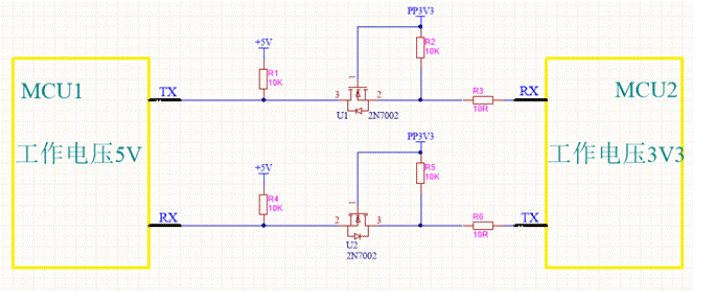


The level bidirectional conversion circuit in Figure 1 can achieve serial communication between MCUs with different VDDs (chip operating voltages).

Figure 1
The core of this circuit lies in the MOS field-effect transistor (2N7002) in the circuit. It has a similar function to a transistor and can be used as a switch to control the on and off of the circuit. However, compared to transistors, MOSFETs have many advantages, which will be discussed in detail later.
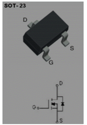
Figure 2 shows the physical 3D diagram and circuit diagram of the MOS transistor. Simply put, to make it a switch, as long as Vgs (conduction voltage) reaches a certain value, pins D and S will conduct. If Vgs does not reach this value, it will cut off.

Figure 2
The function of adding MOS transistors
How to apply 2N7002 to the above circuit and what role does it play? Let‘s analyze it below.

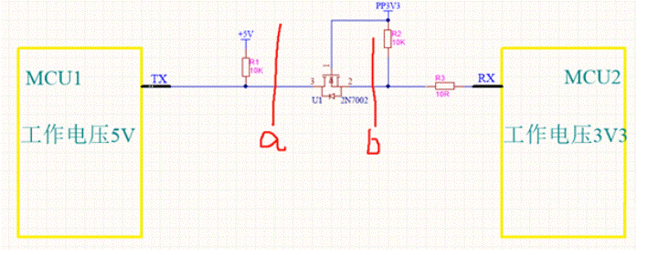
Figure 3
Looking at Figure 3, if you follow lines a and b, cut off the circuit. So the TX pin of MCU 1 is pulled up to 5V, and the RX pin of MCU 2 is also pulled up to 3.3V. The S and D pins of 2N7002 (corresponding to pins 2 and 3 in Figure 3) cut off, which is equivalent to cutting off lines a and b, cutting off the circuit. That is to say, this circuit can deliver the corresponding working voltage to the two MCU pins when 2N7002 is cut off.
1. Analyze data transmission direction from MCU 1 to MCU 2:

Figure 4
1) MCU 1 TX sends a high level (5V), and MCU 2 RX is configured as a serial port receiving pin. At this time, the S and D pins of 2N7002 (corresponding to pins 2 and 3 in Figure 4) are cut off, and the direction of diode 3 → 2 in 2N7002 is not connected. So MCU 2 RX is pulled up by VCC2 to 3.3V.
2) MCU1 TX sends a low level (0V), and at this time, the S and D pins of 2N7002 are still cut off, but the diodes 2 → 3 in 2N7002 are connected in the direction of VCC2, R2, and 2N7002, forming a circuit with MCU1 TX. Pin 2 of 2N7002 is pulled low, and at this time, the MCU 2 RX is 0V. This circuit achieves the effect of level conversion through data transmission from MCU 1 to MCU 2 direction.
2. Analyze data transmission direction from MCU 2 to MCU 1:

Figure 5
1) MCU 2 TX sends a high level (3.3V), and at this time, the voltage difference between Vgs (voltage difference between pins 1 and 2 in Figure 5) is about 0. 2N7002 is cut off, and the direction of diode 3 → 2 in 2N7002 is not connected. At this time, MCU 1 RX pin is pulled up by VCC1 to 5V.
2) MCU2 TX sends a low level (0V), at which point the Vgs (voltage difference between pins 1 and 2 in Figure 5) voltage difference is approximately 3.3V. 2N7002 is conducting, and the direction of diode 3 → 2 in 2N7002 is not connected. The diodes in VCC1, R1, and 2N7002 form a circuit with MCU2 TX. Pin 3 of 2N7002 is pulled low, and at this time, MCU1 RX is 0V.
The circuit transmits data from MCU 2 to MCU 1 direction, achieving the effect of level conversion.
At this point, the analysis of the circuit is complete. It is a bidirectional serial level conversion circuit.
The advantages of MOS transistors
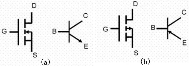
1. The source S, gate G, and drain D of the field-effect transistor correspond to the emitter e, base b, and collector c of the transistor, respectively. Their functions are similar. Figure 5 (a) shows the N-channel MOSFET and NPN type crystal transistor pins, while (b) shows the P-channel MOSFET and PNP type crystal transistor pin correspondence.

Figure 6
2. Field effect transistor is a voltage controlled current device controlled by VGS for ID, while ordinary crystal transistor is a current controlled current device controlled by IB for IC. The amplification factor of MOS pipeline is (transconductance gm) how many amperes can the drain current change when the gate voltage changes by one volt. The crystal transistor has a current amplification factor (beta) β) How much change in collector current can occur when the base current changes by one milliampere.
3. The gate and other electrodes of a field-effect transistor are insulated and do not generate current; During the operation of the transistor, the base current IB determines the collector current IC. Therefore, the input resistance of field-effect transistors is much higher than that of transistors.
4. Only a majority of charge carriers participate in conduction in field-effect transistors; Transistors have two types of carriers, the majority carrier and the minority carrier, involved in conductivity. Due to the significant influence of temperature, radiation, and other factors on the concentration of minority carriers, field-effect transistors have better temperature stability than transistors.
5. When the source and drain of a field-effect transistor are not connected to the substrate, they can be used interchangeably with little change in characteristics. However, when the collector and emitter of a transistor are used interchangeably, their characteristics differ greatly, and the value of b will decrease significantly.
6. The noise coefficient of field-effect transistors is very small, so field-effect transistors should be selected in the input stage of low noise amplification circuits and circuits that require high signal-to-noise ratio.
7. Both field-effect transistors and ordinary crystal transistors can form various amplification and switching circuits. However, field-effect transistors have simple manufacturing processes and excellent characteristics that ordinary crystal transistors cannot match. They are gradually replacing ordinary crystal transistors in various circuits and applications. Currently, field-effect transistors are widely used in large-scale and ultra large scale integrated circuits.
8. High input impedance and low driving power: Due to the silicon dioxide (SiO2) insulation layer between the gate sources, the DC resistance between the gate sources is basically the SiO2 insulation resistance, usually around 100M Ω. The AC input impedance is basically the capacitive impedance of the input capacitor.
Due to the high input impedance, there is no voltage drop on the excitation signal, and it can be driven with voltage, resulting in extremely low driving power (high sensitivity). A typical crystal transistor must have a base voltage Vb to generate a base current Ib in order to drive the generation of collector current. The driving of a crystal transistor requires power (Vb x Ib).
9. Fast switching speed: The switching speed of MOSFETs is closely related to the capacitive characteristics of the input. Due to the presence of capacitive characteristics of the input, the switching speed slows down. However, when used as a switch, it can reduce the internal resistance of the driving circuit and accelerate the switching speed (the input is driven by a "charging circuit" described later, which accelerates the time for capacitive charging and discharging).
MOSFETs rely solely on multi carrier conduction and do not have minority carrier storage effects, resulting in a very rapid turnoff process. The switching time is between 10-100ns, and the operating frequency can reach over 100kHz. Ordinary crystal transistors, due to the storage effect of minority carriers, always have hysteresis in the switch, The impact on the improvement of switching speed (currently, switching power supplies using MOSFETs can easily achieve operating frequencies of 100K/S to 150K/S, which is unimaginable for ordinary high-power crystal transistors).
10. No secondary breakdown: Due to the phenomenon that ordinary power crystal transistors have a positive temperature current characteristic when the temperature rises, the collector current will rise. The increase in collector current will lead to further temperature rise, further temperature rise, and further lead to the vicious cycle of collector current rise.
The voltage resistance (VCEO) of the crystal transistor gradually decreases as the temperature of the transistor increases, resulting in a continuous increase in transistor temperature and a decrease in voltage resistance, ultimately leading to the breakdown of the crystal transistor. This is a destructive thermoelectric breakdown phenomenon that accounts for 95% of the damage rate of the TV switching power supply tube and row output tube, also known as secondary breakdown phenomenon.
MOSFETs have the opposite temperature current characteristics to ordinary crystal transistors, that is, when the tube temperature (or ambient temperature) rises, the channel current IDS actually decreases. For example; A MOSFET switching transistor with IDS=10A, when the VGS control voltage remains constant, IDS=3A at a temperature of 250C. When the chip temperature rises to 1000C, IDS decreases to 2A. This negative temperature current characteristic, which causes a decrease in channel current IDS due to temperature rise, prevents a vicious cycle and thermal breakdown.
That is to say, there is no secondary breakdown phenomenon in MOSFETs. It can be seen that using MOSFETs as switching tubes significantly reduces the damage rate of the switching tubes. In the past two years, after replacing ordinary crystal transistors with MOSFETs in TV switching power supplies, the damage rate of the switching tubes has been greatly reduced, which is also an excellent proof.
11. After conducting, the conduction characteristics of MOS transistors exhibit pure resistance: when a regular crystal transistor is saturated and conducting, it is almost straight through, with an extremely low voltage drop called saturation voltage drop. Since there is a voltage drop, it is; A regular crystal transistor is equivalent to a resistor with extremely low resistance after saturation conduction, but this equivalent resistor is a nonlinear resistor (the voltage on the resistor and the current flowing through it cannot comply with Ohm‘s law). As a switching transistor, MOSFETs also have a resistor with extremely low resistance after saturation conduction.
But this resistor is equivalent to a linear resistor, and its resistance value, voltage drop at both ends, and current flowing through it comply with Ohm‘s law. When the current is large, the voltage drop is large, and when the current is small, the voltage drop is small. After conduction, since it is equivalent to a linear element, the linear element can be applied in parallel. When these two resistors are connected in parallel, there is an automatic current balance effect. So when the power of a MOSFET is insufficient, multiple MOSFETs can be applied in parallel without the need for additional balancing measures (nonlinear devices cannot be directly applied in parallel).
|
Disclaimer: This article is transferred from other platforms and does not represent the views and positions of this site. If there is any infringement or objection, please contact us to delete it. thank you! |


