How to improve the output current driving ability of operational amplifiers
Time:2023-11-18
Views:601
Stability considerations for composite amplifiers
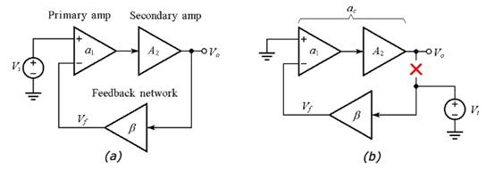
The auxiliary operational amplifier is usually placed inside the feedback loop of the main operational amplifier, as shown in Figure 1 (a). The phase lag introduced by secondary devices often erodes the phase margin of composite amplifiers? m. Therefore, we may have to take appropriate frequency compensation measures.

Figure 1 (a) Block diagram of a composite voltage amplifier. (b) Find the open-loop gain a c and noise gain 1 of the composite amplifier/ β The circuit.
To evaluate the stability of the composite amplifier, we will use the closure rate (ROC) technique. This technology requires us to draw
The overall open-loop gain of the composite amplifier a c (=a 1 × A 2), and
Its noise gain is 1/ β, among β It is the feedback factor of the composite amplifier.
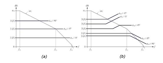
Then we refer to Figure 2 to determine the current situation and estimate accordingly? M.

Figure 2 (a) Frequently encountered phase margin situations, where (b) noise gain independent of frequency 1/ β (jf) and (b) frequency dependent noise gain 1/ β (jf).
To find c and 1/ β, We disconnected the circuit shown in Figure 1 (b), where the output impedance of the secondary amplifier may be much smaller than the impedance presented by the feedback network. Next, we apply the test voltage V t and we
[a_c = frac {V_o}{-V_f}]
Formula 1
And
[frac {1}{eta} = frac {V_t}{V_f}]
Formula 2
Improving the Output Current Driving Ability of Operational Amplifiers
Most operational amplifiers are designed to provide an output current of no more than tens of milliamperes. For example, the ancient 741 operational amplifier can handle an output current of 25 mA. Attempting to exceed this value will activate some internal watchdog circuits to prevent further increase in actual current.
In this case, the operational amplifier will no longer function properly, but at least it can be protected from possible damage caused by excessive power consumption.
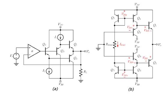
A popular method to improve the output current driving ability of operational amplifiers is to use voltage buffers, as shown in Figure 3 (a).

Figure 3 (a) Use a buffer to increase the output current drive of the operational amplifier. (b) Detailed schematic diagram of the buffer.
The function of Q1 is to provide (or push) current to the load R L, while the function of Q2 is to absorb (or pull) current from R L; Therefore, the Q 1- Q 2 pair is referred to as forming a push pull output stage. Transistors Q 3 and Q 4 have dual purposes:
They provide Darlington type functions to improve the current gain from input to output nodes.
Their base emitter voltage reduction aims to maintain Q1 and Q2 conduction even without any output load, which is why Q1 and Q2 are also referred to as forming AB class output stages. AB class operations can prevent the inherent distortion of B class operations.
For a more detailed analysis, please refer to the complete schematic diagram in Figure 3 (b), where we note the following:
Q 5-Q 6 and Q 7-Q 8 pairs form two current mirrors, sharing the same bias current I BIAS, where
[I_ {BIAS}=frac {(V_ {CC}-V_ {EBp}) - (V_ {EE}+V_ {EBn})} {R_ {BIAS}}]
Formula 3
Q 6 and Q 8 mirror I BIAS and use it to bias Q 3 and Q 4, respectively. As a result, Q 3 and Q 4 generate base emitter voltage drops V EB3 and V BE4.
In response to V EB3 and V BE4, Q 1 and Q 2 generate a base emitter voltage drop V BE1 and V EB2, resulting in
Formula 4 [V_ {BE1}+V_ {EB2}=V_ {EB3}+V_ {BE4}]
Without any load, Q 1 and Q 2 must consume the same current. According to formula 4, the common current consumed by Q 1 and Q 2 must be equal to the current consumed by Q 3 and Q 4, i.e. I BIAS. Therefore, under no load, the collector current meets the condition I C1=I C2=I C3=I C4=I BIAS.
|
Disclaimer: This article is transferred from other platforms and does not represent the views and positions of this site. If there is any infringement or objection, please contact us to delete it. thank you! |


