Common chip issues in analog IP integration
Time:2023-11-07
Views:600
Despite concerns over the end of Moore‘s Law over the past decade, the microelectronics industry continues to adapt to new physical constraints and product requirements through continuous innovation and creativity. Most of the creative energy has been invested in the development of analog, RF, and hybrid signal modules as embedded IPs.


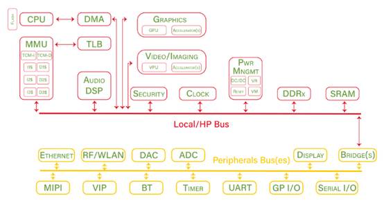
Figure 1 highlights the multimedia SoC design in this block diagram. P2F Semi
The available options for analog/RF/mixed signal IP are both extensive and in-depth. People can find a large number of hardware modules at 7 nm (sometimes even 5 nm) in the following main categories:
PLL and DLL: Provides multiple speed, jitter, and power specifications
DAC and ADC: Resolution from 8 to 24 bits, with speeds up to 300 MSPS
PHY and SerDes: targeting a wide range of market choices, such as wireless (Wi Fi and 5G), network (LAN, WAN, and storage), computing (USB, PCIe, MIPI), and memory (DDR, including G and LP variants, as well as HBM and many others)
Smaller components can be assembled to create personalized analog front-end (AFE), power management functions, and RF modules
The industry continues to make technological advancements to support the endless demand for higher gate counts, lower power consumption, higher performance, and more functionality. This includes triple well isolation, silicon on insulator, P+protection ring, FinFET, and trench isolation. Many of these features have contributed to the surge in analog, RF, and mixed signal IP that we see today. The addition of these substrates also reduces the severity of some complex issues that designers have been facing in the ultra deep submicron field, such as analog noise sources hidden in conversion rates, impedance matching and termination complexity, and circuits that support huge bandwidths.
However, facing the large number of gates placed side by side with analog circuits in SoC designs at 16 nm and below, even novel process enhancements are insufficient. In fact, the signal and power integrity challenges brought by large high-performance digital modules that are very close to analog/RF macros are expanding from chips to packaging and PCBs, both of which are striving to keep up with the progress of silicon technology. SoC designers are increasingly finding themselves forced to expand their work scope to two other areas to ensure that their chip designs run as expected.
This multi part article series explores how embedded simulation and RF IP cores can have a negative impact on chip, packaging, and PCB functionality, with diverse impacts. We will also discuss how to prevent these issues at all three levels and how these solutions complement each other.

Silicon Practice
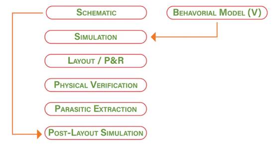
Over the past twenty years, attempts to create unified tools and methodological processes for analog and digital circuit design have thus far proven futile. However, there is a general consensus on the basic outline of the simulation process, as shown in Figure 2.

Figure 2 shows a view of the basic simulation design process. P2F Semi
Although the process may seem quite simple, details determine success or failure.
Analog circuits are very sensitive to the layout and wiring of the circuit. Design rules (wiring and through-hole spacing, differential signals, and additional grounding pins) help to avoid or at least reduce substrate coupling and proximity effects that can cause EMI problems. This is why Design Rule Check (DRC) is a part of the physical verification work after layout. Layout and Schematic (LVS) checks are also part of the same step of verifying expected connectivity.
The extraction of parasitic parameters directly affects the identification of potential coupling sources, and reverse annotation of parasitic parameters often leads to changes in the schematic and layout. Unfortunately, this will affect timing, dynamic range, load, gain, and power, and result in a completely new set of parasitic effects. Therefore, returning to the iterative cycle at the beginning of the design process is a tragic necessity, which is why simulation design is considered more like an art rather than a science.
Integration of simulation blocks
Therefore, integrating the final simulation module into the entire ASIC/SoC design will bring a series of new problems. For digital and analog circuit modules, chip layout planning will be limited by the position, pin layout, I/O position, critical path, power and signal distribution, as well as chip size and aspect ratio of each module. The fact that analog IP is particularly sensitive to most of these issues, and the fact that analog modules are also hard MAC, complicates all of the above issues.
Once the module of the chip is placed, the wiring practice involves first implementing all critical paths, whether analog or digital. However, when non critical paths are involved, analog signals should take priority. In addition, regardless of whether the given analog signal is crucial or not, all analog wiring requires special consideration in matching parasitic effects, reducing coupling effects, and avoiding excessive IR voltage drop. It is achieved by using various shielding techniques for analog signal routing, keeping the routing short, and returning the signal path through direct routing, differential signaling, and other routes.
In addition to these extensive methods of integrating analog content on chip, different categories of analog circuits may also require special attention. DAC and ADC are perfect examples.
When using DAC or ADC, in addition to its resolution and sampling rate, there are also some design considerations, such as its specification signal-to-noise ratio (SNR), significant bit (ENOB) rating, and power consumption. Following the Nyquist sampling theorem (which states that sufficient digital reproduction of analog signals requires sampling at a sampling rate exceeding twice the analog F max) inherently poses bandwidth, power consumption, and bit synchronization challenges for high-performance applications.
From a sampling perspective, wireless is particularly problematic, while audio typically requires resolution. This is where parameters such as ENOB have special correlations. Regardless of the advertising resolution of a given DAC or ADC, pushing such blocks past their ENOB will reduce their SNR performance, potentially having a significant impact on the true usefulness of the block.
Importantly, the design and integration of analog modules into SoC or ASIC environments are not as "clean" and predictable as the digital parts of chips in engineering work. Experience, flexibility, and adaptability are the determining factors for success.
|
Disclaimer: This article is transferred from other platforms and does not represent the views and positions of this site. If there is any infringement or objection, please contact us to delete it. thank you! |


