All information about the reverse phase buck boost converter
Time:2023-10-01
Views:652
All information about the reverse phase buck boost converter is based on the switch mode voltage conversion of inductors, which is a fundamental technique for circuit designers. It enables us to achieve buck and boost regulation through efficient and compact circuits without introducing too much complexity in the process.
I introduced buck and boost regulators in previous articles, and today we will learn about another basic switching regulator topology: an inverted buck boost converter.
When I use the term "basic" in this situation, I refer to a circuit composed of an output capacitor, an inductor, a switch, and a diode. I am mentioning this point now to explain why this article only introduces the reverse phase buck boost architecture and does not include the four switch buck boost architecture.
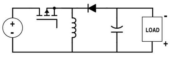
The basic layout of the inverter buck boost converter is shown in Figure 1. This circuit accepts a positive input voltage and generates a negative output voltage, which can be greater or less than the input voltage.

Figure 1. General topology of the inverter buck boost converter.
Now is the time for me to create an implementation in LTspice.
Do you want to review the basic knowledge before delving deeper into it? Read ‘What is a switching regulator?‘ and review the general concepts related to DC-DC converters.
LTspice circuit design
Although I won‘t gradually guide you through the schematic design process this time, I would like to briefly comment on a few aspects.
For my step-down converter schematic, I adopted a formal method that utilizes formulas and performance specifications to determine component values. For boost converters, I have studied more example circuits and prioritized the practical goal of maintaining reasonable inductor sizes.
However, for this buck boost converter, I rely on intuition and repeated experimentation. There are multiple methods for designing the power stage of switch mode power supply (SMPS). Formula and data table suggestions are a great starting point, but don‘t be afraid to try.
Please make sure to carefully check your work. At first, LTspice was unable to successfully run the simulation of the circuit, and I finally realized that the current source was pointing in the wrong direction! Please remember that the V OUT of the reverse phase step-down boost circuit is negative, so the load current flows upwards from the grounding node.
The final version of my buck boost schematic is shown in Figure 2. We will first use it to check the basic operation of the inverter buck boost converter, and then conduct simulations for more detailed analysis.
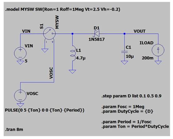
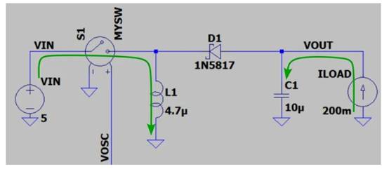
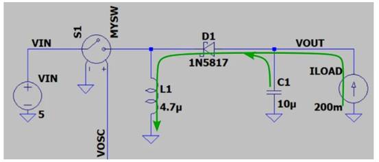

Figure 2. Inverted buck boost converter implemented in LTspice.
Basic Operation of Inverted Step-down Boost Converter
Like the previous converter topology, we will analyze the buck boost converter in two different operating stages: when the switch conducts current (on state), and when the switch blocks current (off state). We will start from the open state.
On state

Figure 3. The current flowing through the step-down boost converter in the connected state.
Figure 3 shows the path of current through the circuit when the switch is on: when the switch is on, the current flows from the input power supply through the inductor and then to the ground.
This figure shows the current flowing through the reverse phase step-down boost converter in the on state.
The inductor is charging - its current is increasing. Meanwhile, the load current is completely provided by the output capacitor, and we assume that the output capacitor has been charged to the output voltage. It flows upwards because V OUT is negative and therefore below ground potential. When we discuss the off state, we will understand why the output capacitor is charged to negative voltage.
Due to the negative V OUT and the voltage at the terminal on the inductor being approximately equal to V IN, the diode is biased in the opposite direction. However, due to the voltage polarity involved, the current naturally flows from the input side to the output side. The direction of the diode can prevent this situation from happening.
Closed state

Figure 4 shows the current path in the off state.
This figure shows the current flowing through the reverse phase step-down boost converter in the off state.
Figure 4. Current flowing through the step-down boost converter in the off state.
When the switch is turned on, the inductor attempts to maintain a consistent current. This causes a voltage drop at the terminals above it until the diode is biased forward. Once the diode is turned on, the inductor serves as the source of load current; It also draws current through the capacitor, so that the voltage at the terminals on the capacitor must be lower than the ground voltage. When the capacitor is charged to negative voltage, V OUT becomes negative.
|
Disclaimer: This article is transferred from other platforms and does not represent the views and positions of this site. If there is any infringement or objection, please contact us to delete it. thank you! |


