Low voltage motor drive design
Time:2023-09-25
Views:673
This application note introduces the design of a low-voltage motor driver using n-channel dual MOSFETs in surface mount packaging. It describes the design using different voltage applications, as well as the adaptive MOSFET gate driver, which is the third method for driving dual n-channel half bridges.
The low-voltage motor driver uses two basic MOSFET configurations: n-channel half bridge and p and n-channel (complementary) half bridge. The main advantage of the complementary method is the simplicity of its gate drive circuit, as described in Vishay Siliconix Application Note AN90-4. When n-channel MOSFETs are used for high side (or "upper") switches, gate drive signals require level conversion, resulting in increased complexity and cost.
5V application
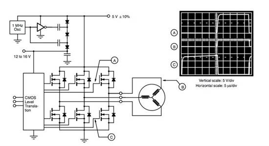
In Figure 1, the charge pump circuit is used to boost the 5 V power supply (actually 4.5 V) to a voltage sufficient to directly drive the upper and lower MOSFET gates.

5V, three-phase motor drive
The rated voltage of the lower n-channel device and providing at least 7.5 V gate enhancement voltage for the upper n-channel MOSFET. The ‘rail to rail‘ drive takes into account input level changes (4.5 to 5.5 V) and charge pump losses, resulting in a power supply voltage range of approximately 12 to 16 V. This voltage range safely leads to a slightly lower impedance of lower devices at the 20-V gate source. However, in motor drive, the total impedance (one upper MOSFET plus one lower MOSFET) is usually more important than symmetry.
12V application
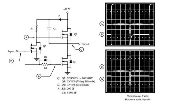
If dynamic gate drive technology is acceptable, it can greatly simplify intermediate low-voltage applications (approximately 12V). Bootstrap capacitor arrangement is a simple and inexpensive method that can provide the voltage required to drive the high side gate (Figure 2). Within a relatively narrow voltage range (approximately 10 to 20 V), simple passive pull-up (R1) values can be selected to provide fast conversion rates and tolerable switching losses. For working voltages above 20V, it may be necessary to use an active pull-up level shifting device, and a Zener diode should be used to clamp the gate source of Q2 to ensure that the V GS rating is not violated. When using this technology, operating voltage below approximately 10 V may result in insufficient Q2 gate drive. The voltage stored in the bootstrap capacitor is equal to 10V (power supply voltage) minus the diode voltage drop, and then minus the MOSFET voltage drop (load current xrDS (on Q1)). The voltage is further reduced due to charge, and charge transfer is necessary to fully enhance the gate of Q2, and the voltage will decay over time due to the leakage current flowing through D1 and Q3.

12V motor drive
In Figure 2, the inputs of the lower MOSFET (Q1) and level conversion MOSFET (Q3) are connected together. The bootstrap arrangement cannot completely eliminate the use of commutation or modulation sequences that close two output devices, and it is necessary to turn on Q1 before turning on Q2 to recharge the bootstrap capacitor. Q2 cannot be maintained indefinitely, and the inherent "dynamic" nature of the bootstrap makes it unusable in certain motor drive applications. But for many others, it can provide technically acceptable and highly cost-effective solutions.
12V to 36V applications
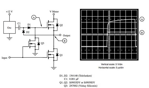
A simple, low component charge pump circuit can provide static operation and tolerable switching time for medium voltage applications. The charge pump circuit shown in Figure 3 has been reduced to a few components, and it is assumed that the system 12V power supply can be used to drive the grounded reference MOSFET gate and oscillator. The oscillator frequency much higher than the required switching frequency will utilize a small charge pump capacitor (C1) to charge the high side MOSFET gate in a short period of time. In this example, in order to achieve a 20kHz switching frequency and tolerable switching losses, a 2MHz oscillator and 0.001 were selected μ F charge pump capacitor to obtain an output rise time of 500ns.

12 to 36 V motor drive
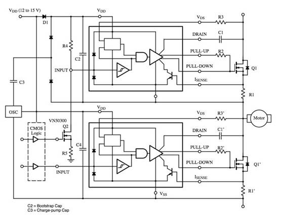
The Si9910DY adaptive MOSFET gate driver (Figure 4) provides a third method of driving a dual n-channel half bridge. Although Si9910 is designed to drive MOSFETs at higher power levels, it has proven to be a highly cost-effective solution for low-power systems (compared to discrete solutions).

In the integrated MOSFET gate driver, Si9910 provides low output impedance while consuming less than 1 A of power current when turned on (output high level). This enables the driver to refer to the source of the high side switch and be powered by a bootstrap capacitor, charge pump, or a combination of both. Combining Si9910 with the peak current capability of a bootstrap capacitor can achieve fast and efficient conversion rates. Adding a small charge pump will overcome conduction state leakage loss, thereby providing continuous (static) operation of high side output devices. Si9910 also provides methods for di/dt, dv/dt, and direct current control, as well as undervoltage and catastrophic current protection.
|
Disclaimer: This article is transferred from other platforms and does not represent the views and positions of this site. If there is any infringement or objection, please contact us to delete it. thank you! |


