RC buffer design for motor drivers
Time:2023-09-14
Views:697
Appropriate RC buffer design
When switching high current through external power MOSFETs to reverse the BLDC motor, ringing may occur, leading to issues such as electromagnetic interference (EMI), circuit jitter, excessive power dissipation, and component overstress. This is usually caused by parasitic inductance and capacitance in printed circuit boards (PCBs), especially in the high current carrying phase network between the high and low side MOSFETs. The inductor and capacitor form an inductor capacitor (L-C) oscillation circuit, which generates resonance during switching events.
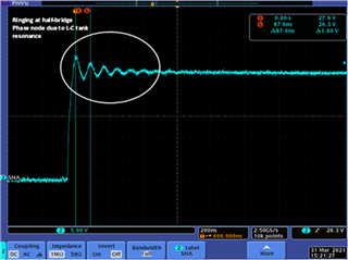
Figure 1- Ringing at the motor phase output due to L-C resonance
To alleviate ringing in the phase output, a simple resistor capacitor (R-C) buffer circuit can be used to "buffer" or suppress oscillations. By eliminating oscillations, voltage overstress can be reduced, thereby reducing potential EMI and extending the lifespan of MOSFETs. The R-C buffer should be placed parallel to the drain and source connectors of each MOSFET as much as possible.
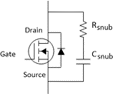
Figure 2- RC buffer
To calculate the resistor (Rsnub) and capacitor (Csnub) values of the R-C buffer circuit, we will use a 7-step program to change the resonant frequency of the MOSFET ringing to calculate the parasitic capacitance (C0) and inductance (L) of the circuit. After obtaining these values, they can be used to derive the values of the R-C buffer. The example shown uses the RC buffer next to the CSD18540Q5B MOSFET (Qgd=6.8nC) of DRV8343-Q1 EVM.
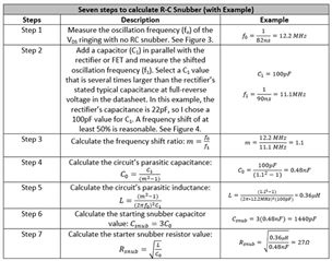
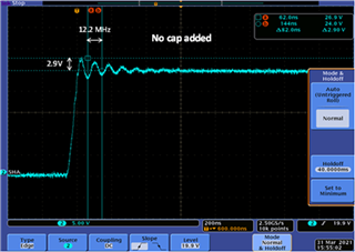
Figure 3- Measurement of VDS ringing fo without RC buffer
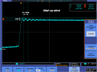
Figure 4- f1 of VDS when measuring C0=100pF
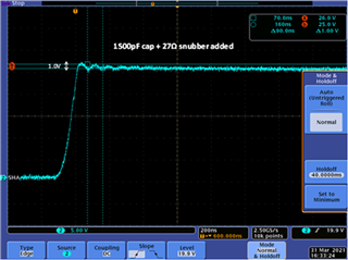
5- Use the calculated RC buffer value to suppress MOSFET ringing
Figure 5 shows the peak reduction and suppression effect of the calculated R-C buffer value. You can increase or decrease the ringing by changing the Csnub value. The higher the value of Csnub, the stronger the ability to reduce the amplitude of voltage spikes, but the greater the power loss in Rsnub.
Alternatively, you can reduce the power dissipation in Rsnub by reducing Csnub, but the ringing will increase. You must balance between acceptable voltage ringing amplitude and Rsnub loss.
If there is a positive or negative voltage transient in the VDS switch event after buffering out the ringing effect, you can reduce the pulling current entering the MOSFET gate or the pouring current from the MOSFET gate. This will increase the rise and fall time of the MOSFET switch and reduce the maximum transient peak. When turning off MOSFETs, it is important to monitor negative voltage transients so that they do not exceed any maximum negative transient specifications of the gate driver device.
|
Disclaimer: This article is transferred from other platforms and does not represent the views and positions of this site. If there is any infringement or objection, please contact us to delete it. thank you! |


