EMI Suppression in Microcontroller Packaging
Time:2023-09-02
Views:717
The control of EMI permeates every corner of circuit design, and there are also methods to prevent EMI in the packaging of IC chips. This article will introduce the role of packaging features in EMI control.
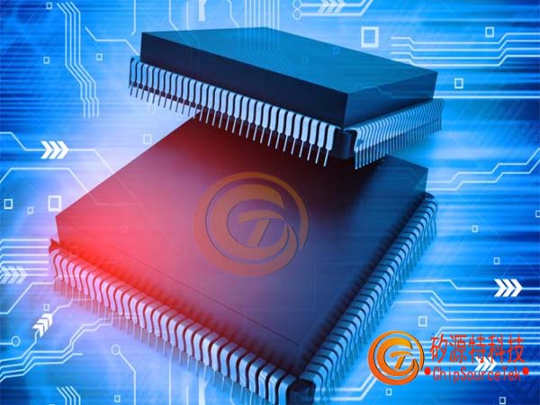
IC packaging typically includes silicon based chips, a small internal PCB, and solder pads. The silicon based chip is installed on a small 64PCB, and the connection between the silicon based chip and the solder pad is achieved through binding wires. In some packages, it can also be directly connected to the small PCB to achieve the connection between the signal and power supply on the silicon based chip and the corresponding pins on the sink package, thus achieving the external extension of the signal and power nodes on the silicon based chip. Therefore, the transmission path of the power and signal of the sink includes the filling chip, the connection between the chip and the small PCB, the PCB wiring, and the input and output pins of the sink package. The control of capacitance and inductance (corresponding to electric and magnetic fields) largely depends on the design of the entire transmission path, and certain design features will directly affect the capacitance and inductance of the entire IC chip packaging.
Let‘s first look at the connection between the silicon based chip and the internal small circuit board. Many sink chips use binding wires to connect the silicon based chip to the internal small circuit board, which is a very thin 6t wire between the silicon based chip and the internal small circuit board. The reason why this technology is widely used is because the thermal expansion coefficient (CU) of silicon based chips and internal small circuit boards is similar. The chip itself is a silicon based device, and its thermal expansion coefficient is significantly different from that of typical PCB materials such as epoxy resin. For example, if the electrical connection point of a silicon based chip is directly installed on an internal small PCB, then after a relatively short period of time, changes in the internal temperature of the IC package will cause thermal expansion and contraction, and this type of connection will fail due to fracture. Binding wire is a wiring method that adapts to this special environment and can withstand large bending deformations without being easily broken.
The problem with using binding wires is that an increase in the current loop area of each signal or power line will lead to an increase in the inductance value. The excellent design for obtaining a lower inductance value is to achieve direct connection between the silicon based chip and the internal PCB, which means that the connection point of the silicon based chip is directly connected to the PCB pad. This requires the selection of a special PCB substrate material that should have an extremely low coefficient of thermal expansion. Choosing this material will lead to an increase in the overall cost of the chip, so chips using this process technology are not common. However, as long as this type of IC that directly connects the silicon based chip to the carrier PCB exists and is feasible in the design scheme, using such an IC device is a better choice.
Generally speaking, reducing inductance and increasing capacitance between the signal and the corresponding circuit or between the power supply and ground are the primary considerations in the process of selecting integrated circuit chips in sink packaging design. For example, small pitch surface mount and large pitch surface mount: Compared to the process, priority should be given to selecting IC chips packaged using small pitch surface mount technology, and both types of surface mount technology package IC chips better than through hole lead type packaging. The BGA packaged sink chip has the lowest lead inductance compared to any commonly used packaging type. From the perspective of capacitor and inductor control, small packaging and finer spacing usually represent an improvement in performance.
An important feature of lead structure design is the allocation of pins. Due to the fact that the values of inductance and capacitance depend on the proximity between the signal or power supply and the return path, it is necessary to consider a sufficient number of return paths.
The power pins and ground pins should be allocated in pairs, and each power pin should have a corresponding ground pin adjacent to it. In this lead structure, multiple power pin and ground pin pairs should be allocated. Both of these features will greatly reduce the loop inductance between the power supply and ground, helping to reduce voltage transients on the power bus, thereby reducing EAdI. Due to customary reasons, many IC chips in the market do not fully follow the above design rules. However, IC designers and manufacturers deeply understand the advantages of this design method, so IC manufacturers pay more attention to power supply connection when designing and releasing new IC chips.
Ideally, it is necessary to assign an adjacent signal return pin (such as a ground pin) to each signal pin. The actual situation is not like this, as many IC manufacturers adopt other compromise methods. In BGA packaging, an effective design method is to set a signal return pin at the center of each group of eight signal pins. In this pin arrangement, each signal differs by only one pin from the signal return path. For square flat package (QFP) or other gull wing (Gullw cut g) style ICs, it is not practical to place a signal return path at the center of the signal group. Even so, it is necessary to ensure that a signal return pin is placed every 4 to 6 pins. It should be noted that different sink process technologies may use different signal return voltages. Some ICs use ground pins (such as TIL devices) as the return path of the signal, while others use power pins (such as the vast majority of ECI devices) as the return path of the signal, while others use both power pins and ground pins (such as most CMoS devices) as the return path of the signal. Therefore, design engineers must be familiar with the logic series of IC chips used in the design and understand their relevant working conditions.
The reasonable distribution of power and ground pins in IC chips can not only reduce EMI, but also greatly improve the ground bounce effect. When the device driving the transmission line attempts to pull it down to the logic low, the ground bounce reflection still maintains the transmission line above the logic low closed level, which may cause circuit failure or malfunction.
Another important issue to pay attention to in IC packaging is the internal PCB design of the chip, which is usually the largest component of the IC packaging. If strict control of capacitance and inductance can be achieved in the internal PCB design, it will greatly improve the overall EMI performance of the system. If this is a two-layer PCB board, at least one side of the PCB board is required to be a continuous ground layer, and the other side of the PCB board is the wiring layer for power and signal. A more ideal scenario would be a four layer PCB board, with the middle two layers being the power and ground layers, and the outer two layers serving as the signal wiring layers. Due to the fact that the PCBs inside the package are usually very thin, the design of a four layer board structure will lead to two high capacitance and low inductance wiring layers, which are particularly suitable for power distribution and strict control of input and output signals entering and exiting the package. A low impedance planar layer can greatly reduce voltage transients caused by power bus failures, thereby greatly improving EMI performance. This controlled signal line not only helps to reduce EMI, but also plays an important role in ensuring the integrity of inbound and outbound signals.


|
Disclaimer: This article is transferred from other platforms and does not represent the views and positions of this site. If there is any infringement or objection, please contact us to delete it. thank you! |


