The design details of MOS transistor driver circuits that engineers must know
Time:2023-08-30
Views:718
It is generally believed that MOSFETs are voltage driven and do not require driving current. However, there is a junction capacitor between the G and S stages of the MOS, which makes driving the MOS less simple.
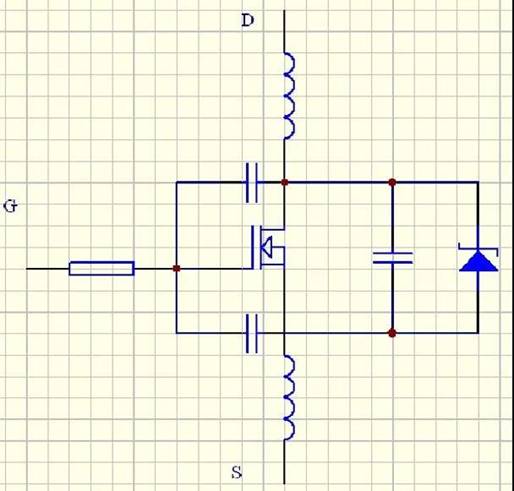


If ripple and EMI requirements are not considered, the faster the MOS transistor switching speed, the better. The shorter the switching time, the smaller the switching loss. In switching power supplies, the switching loss accounts for a large part of the total loss. Therefore, the quality of the MOS transistor driving circuit directly determines the efficiency of the power supply.
For a MOS transistor, the shorter the time it takes to pull the voltage between GS from 0 to the opening voltage of the transistor, the faster the MOS transistor will open. Similarly, if the GS voltage of the MOS transistor is reduced from the opening voltage to 0V in a shorter time, the speed at which the MOS transistor turns off will also be faster.
From this, we can know that if we want to raise or lower the GS voltage in a shorter time, we need to provide a larger instantaneous driving current to the MOS gate.
The commonly used method of directly driving MOS with PWM chip output or amplifying MOS with a transistor before driving MOS actually has significant drawbacks in instantaneous driving current.
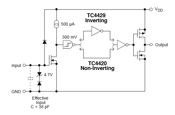
A better method is to use specialized MOSFET driver chips such as TC4420 to drive MOSFETs. These chips generally have a large instantaneous output current and are also compatible with TTL level input. The internal structure of MOSFET driver chips is as follows:

Points to pay attention to in MOS driver circuit design:
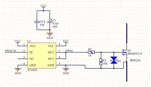
Because the driving circuit wiring will have parasitic inductance, and the parasitic inductance and MOS transistor junction capacitance will form an LC oscillation circuit. If the output end of the driving chip is directly connected to the MOS transistor gate, there will be significant oscillations on the rising and falling edges of the PWM wave, leading to rapid heating or even explosion of the MOS transistor. The general solution is to connect a resistance of about 10 ohms in series at the gate to reduce the Q value of the LC oscillation circuit and quickly attenuate the oscillations.
Due to the extremely high input impedance of MOS gates, even a small amount of static electricity or interference can cause MOS transistors to mislead. Therefore, it is recommended to parallel a 10K resistor between MOS transistors G and S to reduce the input impedance.
If you are concerned about the interference coupling on nearby power lines causing instantaneous high-voltage breakdown of MOS transistors, you can connect an additional 18V TVS transient suppression diode in parallel between the GS.
TVS can be considered as a fast reaction voltage regulator, which can withstand power of up to several hundred to several kilowatts in an instant and can be used to absorb instantaneous interference pulses.
MOS transistor driver circuit reference

Wiring Design of MOS Tube Driver Circuit
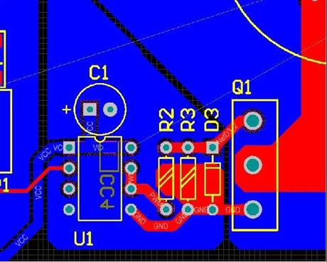
The loop area of the MOS transistor driver circuit should be as small as possible, otherwise foreign electromagnetic interference may be introduced.
The bypass capacitor of the driver chip should be as close as possible to the VCC and GND pins of the driver chip, otherwise the inductance of the wiring will greatly affect the instantaneous output current of the chip.

Common MOS transistor driving waveforms

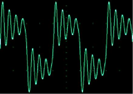
If there is such a round and irregular waveform, wait for a nuclear explosion. A large portion of the time, the pipes work in the linear region, resulting in extremely large losses.
In general, this situation is when the wiring is too long, the inductance is too high, and the gate resistance cannot save you. You can only redraw the board.

High frequency ringing severely disfiguring square waves.
When the oscillation is severe on the rising and falling edges, the pipe usually dies instantly, similar to the previous situation, entering the linear zone.
The reason is similar, mainly due to wiring issues. Fat and round pig waves.
The rising and falling edges are extremely slow, which is caused by impedance mismatch.
The chip‘s driving ability is too poor or the gate resistance is too high.
Decisively switch to a high current driver chip and adjust the gate resistance to a smaller one, which will be fine.
The triangular waves born in Fangbo and their family, with swollen faces filled with sine waves.
The impedance of the driving circuit is too high. This is the inevitable killing wave of the pipe. The solution is the same as above.

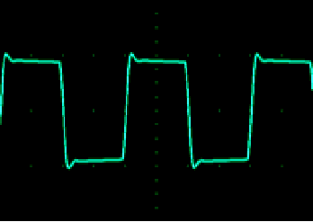
The popular face shape is a beloved square wave.
The high and low levels are clearly defined, and the level can now be called the level because it is flat. The edge is steep, the switching speed is fast, the loss is very small, and there is slight oscillation. It is acceptable, but the tube cannot enter the linear zone. If you have OCD, you can adjust the gate resistance appropriately.
The handsome and square wave with no ringing, no spikes, and no linear loss is the perfect waveform.
|
Disclaimer: This article is transferred from other platforms and does not represent the views and positions of this site. If there is any infringement or objection, please contact us to delete it. thank you! |


