The matter of RF wiring and ground
Time:2023-08-05
Views:780
Let‘s give an example. We will conduct RF line simulation on multi-layer circuit boards. In order to make a better comparison, the simulated PCB will be divided into two boards before and after surface laying for simulation comparison; The PCB file with unpaved surface is shown in Figure 1 (two line widths):
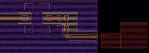
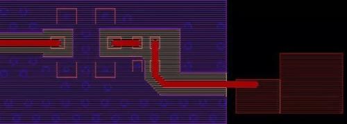
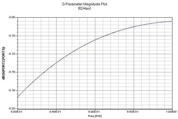
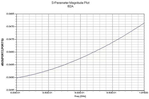

Figure 1a: RF line with a width of 0.1016 mm (before surface paving)

Figure 1b: Radio frequency line with a width of 0.35 mm (before surface paving)
Figure 1: PCB with unpaved surface
Firstly, import two boards with different line widths (before surface paving) from ALLEGRO into SIWAVE, and add a 50 Ω port on the target line. For different line widths of 0.1016mm and 0.35mm, our simulation results are shown in Figure 2. The curve shown in the figure is S21, and the simulation frequency range is 800MHz-1GHz.

Figure 2a: S21 with unpaved surface (line width 0.1016mm)

Figure 2b: S21 with unpaved surface (line width 0.35mm)
Figure 2: S21 with unpaved surface
As can be seen from the figure, in the range of 800MHz-1GHz, the simulation data shows the order of magnitude of one to two digits after the Decimal separator. The loss of 0.35mm is one order of magnitude smaller than that of 0.1016mm line, because the characteristic impedance of 0.35mm line width is close to 50 Ω under the stacking condition of the board. Therefore, it indirectly verifies that our impedance calculation (constrained by line width) has a certain effect.
Next, we conducted the same simulation (800MHz-1GHz) after surface paving, and the imported PCB file is shown in the following figure.
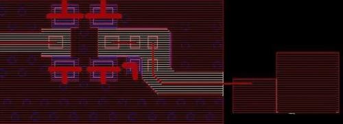

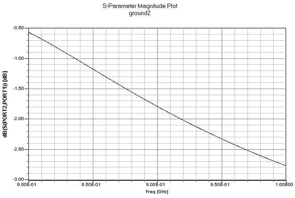
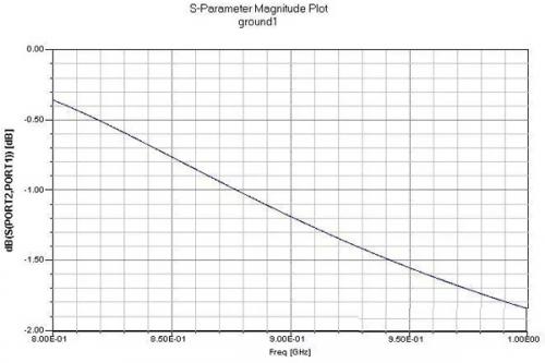

Figure 3a: 0.1016 mm RF line (surface paving)

Figure 3b: 0.35 mm RF line (surface paving)
Figure 3: PCB with surface laid on the ground
The simulation results are shown in the following figure:

Figure 4a: S21 (0.1016mm) after surface paving

Figure 4b: S21 (0.35mm) after surface paving
Figure 4: S21 after the surface layer is laid on the ground
As shown in the figure, the simulated data shows that the line loss of the transmission line is already on the order of 1-2 dB, and of course, the loss of 0.35 mm is significantly smaller than that of 0.1016 mm. Another obvious phenomenon is that compared to the simulation results without paving the ground, the loss increases as the frequency increases from 800MHz to 1GHz.
We can obtain the following result from the simulation results:
1. It is best to route the RF cable at 50 ohms to reduce line loss;
2. The surface paving actually couples a portion of RF signal energy to the ground, causing certain losses. Therefore, there should be some attention to the flooring of the PCB surface. Try to stay away from the RF line as much as possible. Engineering experience is greater than 1.5 times the line width.
|
Disclaimer: This article is transferred from other platforms and does not represent the views and positions of this site. If there is any infringement or objection, please contact us to delete it. thank you! |


