Discussion on Mosfet Drive Circuit
Time:2023-07-30
Views:790
MOSFETs are widely used in switching power supplies due to their low internal resistance and fast switching speed. The driver of MOSFETs often selects the appropriate circuit based on the parameters of the power supply IC and MOSFET. Let‘s explore the driving circuit of MOSFETs used in switching power supplies together.
When designing switching power supplies using MOSFETs, most people consider the conduction resistance, maximum voltage, and maximum current of MOSFETs. But many times, only these factors are considered, and such a circuit may work properly, but it is not a good design solution. More specifically, MOSFETs should also consider their own parasitic parameters. For a certain MOSFET, its driving circuit, peak current output from the driving pins, rise rate, etc., will all affect the switching performance of the MOSFET.
After selecting the power IC and MOS transistor, it is particularly important to choose the appropriate driver circuit to connect the power IC and MOS transistor.
A good MOSFET driver circuit has the following requirements:
(1) At the moment when the switch is turned on, the driving circuit should be able to provide sufficient charging current to quickly increase the voltage between the MOSFET gate and source to the required value, ensuring that the switch can be turned on quickly without high-frequency oscillation on the rising edge.
(2) The driving circuit can ensure stable and reliable conduction of MOSFET gate source voltage during the switch conduction period.
(3) The turn-off instantaneous driving circuit can provide a path with as low impedance as possible for rapid discharge of MOSFET gate source capacitor voltage, ensuring that the switch can be quickly turned off.
(4) The driving circuit structure is simple and reliable, with low losses.
(5) Apply isolation according to the situation.
The following introduces the commonly used MOSFET driver circuits in several module power supplies.
1: Power IC directly drives MOSFETs

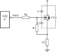
Figure 1 IC Direct Drive MOSFET
Direct driving of power IC is the most commonly used and simplest driving method for us. When using this driving method, we should pay attention to several parameters and their effects. Firstly, take a look at the power supply IC manual. The maximum driving peak current is often different due to different chips having different driving capabilities. Secondly, understand the parasitic capacitance of MOSFETs, as shown in the values of C1 and C2 in Figure 1. If the values of C1 and C2 are relatively large, the energy required for MOS transistor conduction is relatively large. If the power supply IC does not have a relatively large driving peak current, the speed of transistor conduction is relatively slow. If the driving capacity is insufficient, high-frequency oscillation may occur on the rising edge, and even reducing Rg in Figure 1 cannot solve the problem! Factors such as IC driving capability, MOS parasitic capacitance size, and MOS transistor switching speed all affect the selection of driving resistance value, so Rg cannot be infinitely reduced.
2: When the power IC driving capacity is insufficient
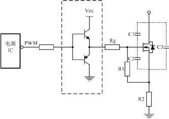
If the parasitic capacitance of MOS transistor is relatively large and the internal driving capability of the power IC is insufficient, it is necessary to enhance the driving capability on the driving circuit. Totem pole circuits are often used to increase the driving capability of the power IC, as shown in the dashed box in Figure 2.

Figure 2 totem pole driven MOS
The function of this driving circuit is to enhance the current supply capacity and quickly complete the charging process of the input capacitor charge of the gate. This topology increases the time required for conduction, but reduces the turn-off time. The switch can be quickly turned on and avoid high-frequency oscillation of the rising edge.
3: Driving circuit acceleration MOS transistor turn off time
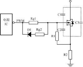
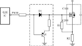
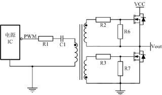

Figure 3 Accelerated MOS shutdown
The turn-off instantaneous driving circuit can provide a path with as low impedance as possible for the rapid discharge of MOSFET gate source capacitor voltage, ensuring that the switch can be quickly turned off. In order to quickly discharge the capacitance voltage between the gate source electrodes, a resistor and a diode are often connected in parallel on the driving resistor, as shown in Figure 3. Among them, D1 is commonly used as a fast recovery diode. This reduces the shutdown time and also reduces the loss during shutdown. Rg2 prevents excessive current from burning out the power IC during shutdown.

Figure 4 Improved Accelerated MOS Shutdown
The totem pole circuit introduced in the second point also has an accelerating shut-off effect. When the driving capacity of the power IC is sufficient, improving the circuit in Figure 2 can accelerate the MOS transistor turn off time, resulting in the circuit shown in Figure 4. It is common to use a transistor to discharge the capacitance voltage between the gate and source electrodes. If there is no resistance at the emitter of Q1, when the PNP transistor is on, the capacitance between the gate and source electrodes is short circuited to discharge the charge in the shortest possible time and minimize the cross loss during shutdown. Compared with the topology in Figure 3, another advantage is that the current on the charge discharge of the gate source capacitor does not pass through the power IC, which improves reliability.
4: Driving circuit acceleration MOS transistor turn off time

Figure 5 Isolation Drive
In order to meet the driving requirements of high-end MOS transistors as shown in Figure 5, transformer driving is often used, and sometimes transformer driving is also used to meet safety isolation requirements. The purpose of R1 is to suppress the parasitic inductance on the PCB board and form LC oscillation with C1, while the purpose of C1 is to isolate DC through AC while also preventing magnetic core saturation.
In addition to the above driving circuits, there are many other forms of driving circuits. There is no best driving circuit for a variety of driving circuits, only by combining specific applications and selecting the most suitable driving circuit.
|
Disclaimer: This article is transferred from other platforms and does not represent the views and positions of this site. If there is any infringement or objection, please contact us to delete it. thank you! |


