Component packaging
Time:2023-06-28
Views:876
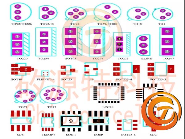
Part packaging refers to the appearance and location of solder joints indicated when the actual part is soldered onto a circuit board. It is a pure spatial concept, so different components can share the same part packaging, and the same component can also have different part packaging. Like resistors, there are traditional pin in type components, which have a larger volume and require drilling holes on the circuit board to accommodate the components. After drilling, the components are inserted and then soldered in a tin furnace or spray soldering (which can also be done by hand), resulting in higher costs. Newer designs use small surface mount devices (SMD), which do not require drilling holes. Instead, a steel film is used to pour semi molten solder paste into the circuit board, and then the SMD components are placed on top to be soldered onto the circuit board. We mentioned earlier about part packaging, except for the DEVICE. Except for the components in the LIB library, the components in other libraries already have fixed component encapsulation, because the components in this library have various forms:
Taking transistors as an example, it can be explained that they are one of the commonly used components in DIVICE. In the LIB library, there is only a simple distinction between NPN and PNP. However, in reality, if it is the 2N3055 of NPN, it may be the TO-3 of the iron shell. If it is the 2N3054 of NPN, it may be the TO-66 or TO-5 of the iron shell. The learned CS9013 includes TO-92A, TO-92B, TO-5, TO-46, TO-52, and so on, which are constantly changing.
Another is resistance. In the DEVICE library, it is also simply called RES1 and RES2, no matter whether it is 100 Ω or 470K Ω. For the circuit board, it is not related to the ohm number at all. The 1/4W and even 1/2W resistors we choose are determined entirely by the power number of the resistance. They can be packaged with AXIAL0.3 components. If the Power number is larger, XIAL0.4, AXIAL0.5, and so on.
The commonly used component packaging is now organized as follows:
Resistive and non-polar dual ended components AXIAL0.3-AXIAL1.0/ Non polar capacitor RAD0.1-RAD0.4/polar capacitor RB.2/.4-RB.5/1.0/
Diode DIODE0.4 and DIODE0.7/quartz crystal oscillator XTAL1/transistor, FET, UJT TO-xxx (TO-3, TO-5)/
Variable resistance (POT1, POT2) VR1-VR5
Of course, we can also open the C:/Client98/PCB98/library/advpcb.lib library to search for the corresponding packaging of the used parts. It is best for you to memorize these commonly used component packages. For these component packages, you can split them into two parts to remember, such as the resistor AXIAL 0.3, which can be disassembled into AXIAL and 0.3, and AXIAL translated into Chinese is axial, 0.3 is the distance between the pads of the resistance on the printed circuit board, which is 300 mil (because in the field of motors, Imperial units are the main units).
Similarly, for non-polar capacitors, RAD0.1-RAD0.4 is also the same; For polar capacitors such as Electrolytic capacitor, their packages are RB. 2/. 4, RB. 3/. 6, etc., where ". 2" is the pad spacing, and ". 4" is the outer diameter of the capacitor cylinder. For transistors, it depends directly on their appearance and power. For high-power transistors, use TO-3. For medium power transistors, use TO-220 if they are flat, TO-66 if they are metal shell. For low-power transistors, use TO-5, TO-46, TO-92A, etc. Anyway, their pins are also long and can be bent slightly. For commonly used integrated IC circuits, there are DIPxx, which is a dual inline component packaging, and DIP8, which is a dual row with 4 pins per row. The distance between the two rows is 300mil, and the distance between the pads is 100mil. SIPxx is a single row packaging. Wait a minute.
It is worth noting that the packaging of transistors and variable resistors is the most headache, and the same packaging may not necessarily have the same pins. For example, for packaging such as TO-92B, usually pin 1 is E (emitter), while pin 2 may be either B (base) or C (collector); Similarly, pin 3 may be either C or B, and the specific one can only be determined after obtaining the component. Therefore, the circuit software dare not define the pad name (pin name) rigidly. Similarly, Field-effect transistor and MOS transistor can also be packaged in the same way as transistors, which can be used for three pin components. Q1-B, in the PCB, when loading this network table, the node cannot be found (not aligned). Similar problems can also occur on variable resistors; In the schematic diagram, the pins of the variable resistor are 1, W, and 2, respectively, resulting in a network table of 1, 2, and W. In a PCB circuit board, the pads are 1, 2, and 3. When there are these two components in the circuit, the fastest way to modify the difference between PCB and SCH is to directly change the transistor pins to 1, 2, and 3 in the network table after generating the network table; Change the variable resistor to 1, 2, and 3 that have the same appearance as the circuit board components.
The processing of encapsulation is a trivial matter that requires a lot of knowledge but requires a lot of effort. For example, DIP8 is very simple, but some libraries use DIP-8, while others use DIP8 Even for the same packaging structure, there are significant differences in the description of product datasheets among different companies (different file name systems, different name titles, etc.); There are also cases where the same model of device has different pin sorting, and so on. For old devices, such as the inductance you mentioned, there are different specifications (inductance, current) and design requirements (plug-in/SMD). It‘s true that no one can help anyone, and I can‘t even help anyone if I want to. In most cases, I still rely on my own accumulation. This is a confusing problem for people, especially those who are just starting to use this type of software, and it is often difficult to confidently find (or confirm) the corresponding footprint in the data, which is sure to be correct - I have no idea! Actually, it‘s quite normal. I don‘t think there are many ready-made "all-around" libraries; selecting models based on circuit design, finding product information, carefully verifying packaging, and building libraries (components) yourself if necessary. These are all necessary information accumulation for using such software to complete the design. This process is indispensable for anyone. If we can persist, it is estimated that only one or two product designs will be needed to become proficient. The so-called "veteran" are also mostly like this Coming over, even as a ‘house keeper‘ thing. This "endure" is not very easy, but it is necessary.
Resistive and non-polar dual ended components AXIAL0.3-AXIAL1.0
Non polar capacitor RAD0.1-RAD0.4
Polarized capacitor RB.2/.4-RB.5/1.0
Diodes DIODE0.4 and DIODE0.7
Quartz crystal oscillator XTAL1
Transistor, FET, UJT TO-xxx (TO-3, TO-5)
Variable resistance (POT1, POT2) VR1-VR5


|
Disclaimer: This article is transferred from other platforms and does not represent the views and positions of this site. If there is any infringement or objection, please contact us to delete it. thank you! |


