Low voltage reset circuit of transistor
Time:2023-05-13
Views:1032
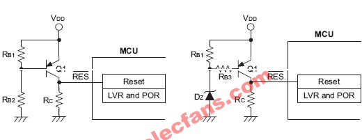
Low voltage reset circuit of transistor

When the voltage of the built-in low-voltage reset circuit is different from the application specifications, an external transistor low-voltage reset circuit can be selected.
It can provide low voltage reset function and is suitable for strong interference environments.
The low voltage reset function is determined by the voltage division between RB1 and RB2, or by the voltage of the voltage regulator diode.
When using RB1 and RB2 voltage sharing, the low voltage reset point is approximately (RB1+RB2)/(2 × RB1), RC resistance value should be greater than RB2/30.
When using a voltage regulator diode, its low voltage reset point is about VZ+0.5V, RB1 is used to set the working point VZ, RC resistance value is preferably greater than 100k Ω, and RB3 resistance value is about 10k Ω.
The position of transistor Q1 on the PCB board is very important, and it is generally required that the collector (C) and emitter (E) of Q1 have the shortest wiring to the RES and VDD pins of the MCU.
|
Disclaimer: This article is transferred from other platforms and does not represent the views and positions of this site. If there is any infringement or objection, please contact us to delete it. thank you! |


