High precision and high edge current detection amplifier monitoring PWM load current
Time:2023-03-20
Views:1142
1、 Working principle
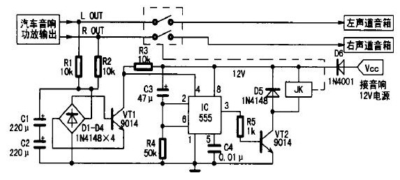
The speaker protection circuit is shown in Figure 1. It mainly consists of a midpoint potential detection circuit, a delay circuit, and a relay. The working process of the circuit is:

Figure 1 Speaker Protection Circuit
"At the moment of turning on the audio power supply, because the voltage at both ends of capacitor C3 cannot suddenly change, it can be considered as a short circuit, and the potential of pins ② and ⑥ of time base circuit 555 is higher than 2/3 Vcc, so 555 is in a reset state. Pin ③ outputs a low level, transistor VT2 is turned off, and the normally open contact of relay JK does not act.". At the same time, a voltage of+12 V is charged to the capacitor C3 through the resistor R4. After a delay of about 5 s (seconds), the potential of the ② and ⑥ pins of 555 decreases to 1/3 Vcc, and 555 is triggered to set. The ③ pin changes from a low level to a high level. The transistor VT2 is turned on, the relay JK is powered on, and the normally closed contact is closed, thereby achieving a delay in connecting the speaker to the power amplifier for a period of time, completely eliminating the impact of high current on the speaker during startup;
When turning off the audio power supply, the+12 voltage quickly disappears, but the amplifier output signal does not immediately disappear, which also avoids the impact noise generated during the shutdown process;
When the midpoint potential is too high (higher than 1.8 V) due to abnormal operation or accidental damage of the power amplifier, the DC voltage is limited by R1 and R2 and sent to C1 and C2 filtering and D1 to D4 rectification. For about 1-2 seconds, transistor VT1 is turned on, pin ④ of 555 changes from high to low, and 555 is directly reset. Pin ③ outputs a low level, transistor VT2 is turned off, relay JK loses power, and the normally open contact jumps open, disconnecting the speaker from the power amplifier circuit, Effectively protects the speaker from damage.
By changing the parameters of R4 and C3, the length of the startup delay time of the speaker protection circuit can be adjusted, generally set to 5 seconds.
2、 Component Selection
The 555 must choose a CMOS time base circuit with very low power consumption. Type 9014 and C1815 low-power plastic encapsulated transistors for VT1 and VT2 require current amplification β> 100. Both D1 and D5 use 1N4148 type silicon switching diodes, and D6 is used for power connection reverse protection. 1N4001 to 1N4007 type silicon rectifier diodes can be selected. Both R1 and R5 use 0.5 W five-color ring metal film resistors. C1 and C2 use high-quality aluminum electrolytic capacitors, and C3 should use tantalum electrolytic capacitors with low leakage and high accuracy, otherwise the delay accuracy will be affected. JK selects a 12 V/7 A duplex relay (one set for each of the left and right channels), such as JZC-22F
3、 Fabrication and commissioning
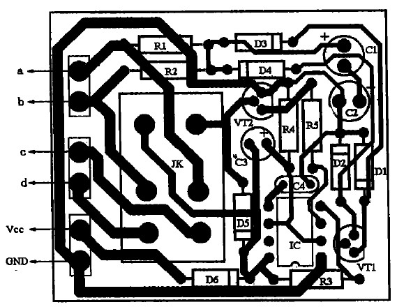
Figure 2 is a PCB diagram of the speaker protection circuit. Its actual size is about 50 × 43 mm。

Figure 2 PCB board diagram
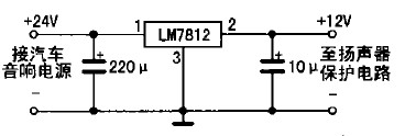
The specific production is as follows: First, cut off the lead between the amplifier output terminal and the speaker box, connect the lead heads a and b to the two sets of output terminals of the amplifier according to the circuit shown in Figure 2, and connect the lead heads c and d to the left and right channel speakers respectively. The power supply for the speaker protection circuit can only be obtained from the radio and amplifier, and cannot be directly obtained from the vehicle 12V power supply, otherwise it will not have the protection effect of turning on/off; If the radio and cassette player equipped with a diesel vehicle (using a 24 V power supply), it is required to add a step-down circuit (as shown in Figure 3) to supply power to the speaker protection circuit to prevent excessive power supply voltage from damaging the IC.

Figure 3 Step-down circuit
|
Disclaimer: This article is transferred from other platforms and does not represent the views and positions of this site. If there is any infringement or objection, please contact us to delete it. thank you! |


