Negative buck converter does not need inductor
Time:2023-02-07
Views:1336
The circuit uses two charge pump devices to reduce the negative voltage. The first generates positive output by doubling and inverting the negative input voltage, and the second acts as an inverter to generate the required negative output. The input and output capability of the circuit depends on the allowable input/output voltage of the selected IC element.
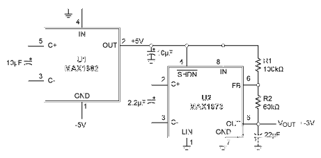
To reduce the negative voltage in low current applications, the non-inductive configuration combines ease of use with a small number of external components. The buck converter can be realized by two charge pump devices. The first generates positive output by doubling and inverting the negative input voltage, and the second acts as an inverter to generate the required negative output. The input and output capability of the circuit depends on the allowable input/output voltage of the selected IC element (Figure 1).

Figure 1. The negative step-down converter (- 5V to - 3V) does not require an inductor.
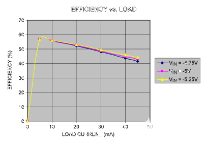
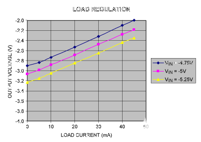
U1 (MAX1682) works as a voltage multiplier, accepts 5V negative input and generates 5V positive output. The regulated inverter (U2, MAX1673) accepts+5V voltage and generates - 3V output. The voltage divider (R1/R2) at the U2 output terminal provides feedback to adjust the output voltage of U2 to the required level (outside V). At the FB input terminal, the threshold voltage is set to zero at the factory. You can use R2 (5V/R1)=- V to select the values of R1 and R2, and their sum should allow a minimum current of 50 μ A. The accuracy of V depends largely on the accuracy of - 5V input. Figure 2 and Figure 3 show the circuit efficiency and output regulation of - 4.75V, - 5V and - 5.25V inputs.

The relationship between the efficiency of the circuit in Figure 1 and the load at the level of - 4.75V, - 5V and - 5.25V is shown in Figure 2. V.

Figure 3. The load adjustment rate of the circuit in Figure 1 at V is - 4.75V, - 5V and - 5.25V.
|
Disclaimer: This article is transferred from other platforms and does not represent the views and positions of this site. If there is any infringement or objection, please contact us to delete it. thank you! |


