Method Analysis of Output Drive Capability of Operational Amplifiers
Time:2023-02-04
Views:1363
When selecting operational amplifier (operational amplifier) in the circuit to achieve a specific function, one of the most challenging selection criteria is the output current or load driving ability. Most of the performance parameters of the operational amplifier are usually clearly given in the data manual, performance chart or application guide. The designer must refer to the output current and other various parameters of the operational amplifier to meet the product performance specified in the data manual. The output current of devices provided by different semiconductor manufacturers and even different devices provided by the same manufacturer are very different, which makes the design and application of operational amplifiers more complex. This article will explain through some examples how to evaluate the driving capacity of the circuit to be designed according to the performance parameters of the operational amplifier, so as to help the designer ensure that the selected product has sufficient load driving capacity in all cases.
What factors affect driving ability
Output drive capability is a function of a series of internal and external settings or conditions. The bias current, drive stage, structure and process of the output stage are all internal factors. Once a device is selected to achieve a specific function, the designer can no longer change these internal conditions that affect the output drive capability. One of the reasons for the poor output driving ability of most low-power operational amplifiers is that the bias current of their output stage is small. On the other hand, high-speed operational amplifiers usually have high driving capacity, which can meet the low resistance requirements of high-speed circuits. High-speed operational amplifiers usually have high power supply working current, which will also improve the output drive capability.
Traditionally, the performance of integrated PNP transistors is worse than that of NPN transistors. In this process, PNP output transistor is lower than NPN β Value means that the output drive capacity will be unbalanced. The operational amplifier with full swing output usually uses the collector of the transistor as the output pin. The poor performance of PNP tube will lead to the poor ability of providing source current than providing sink current. For non-full swing devices, the opposite is true. Because most devices use the emitter output of PNP transistors, which greatly affects the well current characteristics, their ability to output well current is poor. Moreover, when estimating the output current capacity of the device, the performance fluctuation between devices should also be taken into account. Therefore, when selecting devices based on the "typical" data book specification, the designer must also consider the "limit" and "minimum" specifications to ensure that each device used has sufficient driving capacity during production.
In addition to the internal factors listed above, some external factors will also affect the driving ability. Some of them can be controlled to optimize the output drive capability, while the rest are difficult to control. The external factors that affect the output driving capacity are listed below: the output voltage margin relative to the corresponding power supply voltage (the difference relative to the power supply voltage); Input over-drive voltage; Total power supply voltage; DC and AC coupling load; Junction temperature.
The output driving capacity is usually given in the form of output short circuit current. At this time, the manufacturer specifies the current value that can be provided when the output is grounded (1/2 supply voltage in the case of single power supply, called "Vs/2"). The manufacturer may provide two values, one representing the source current (usually preceded by "+") and the other representing the well current (usually preceded by "-"). In applications where the voltage swing on the load is very small, there will be a large voltage difference between the output stage driver and the power supply voltage (source current is V+, leakage current is V -). At this time, users can use this data to effectively predict the performance of this operational amplifier. Imagine that the operational amplifier carries a large load and the load is driven by a voltage close to the ground (or Vs/2 in the case of a single power supply). If the load of the amplification stage is gradually changing, the current that can be supplied to the load will be consistent with the current value given in the "output short circuit current" in the operational amplifier data manual. Once the output begins to change, two situations will occur: the output voltage margin of the operational amplifier decreases; The input over-drive voltage of the operational amplifier is reduced.
The output current provided by the former reason will be reduced, which is also related to the design of the operational amplifier. As described in the latter, the reduction of the over-drive voltage will also cause the reduction of the output current.
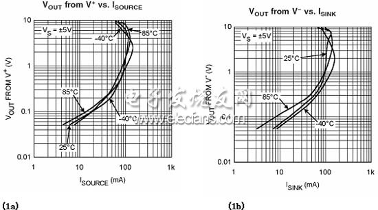
Another more useful method to determine current capacity is to use output current and output voltage diagrams. Figure 1 shows the output current and output voltage of LMH6642 of National Semiconductor Corporation of America. For most devices, the source current (Fig. 1a) and the trap current (Fig. 1b) are usually given a diagram respectively.

Figure 1: Output characteristics of LMH6642.
Using this diagram, we can estimate the current that can be provided for a given output swing operational amplifier. These diagrams are provided by the semiconductor manufacturer to show the relationship between the output current capability of the amplifier and the output voltage.
Please note that in Figure 1, the relationship between "Vout from V+" and output source current and the relationship between "Vout from V -" and output well current are described. One of the reasons for using this method to represent data is that it can be more easily applied to single power supply or dual power supply operation than the output voltage relative to ground. Another reason is that the voltage margin ratio
The power supply voltage of has a much greater impact on the output current. Therefore, for any power supply voltage, even if the exact corresponding conditions can not be found in the data manual, this data manual method can also enable the designer to conduct rough calculation through a set of closest curves.
Figure 1 can be used to predict the voltage swing on a given load. If the coordinate axis is linear, the designer only needs to add a load curve to the characteristic curve in Figure 1. The voltage swing can be determined through the intersection of the two curves. However, as shown in the figure, in many cases, especially when the operational amplifier is full swing output, both coordinate axes use logarithmic coordinates, so that the curve can also have better resolution when the output current is very small and the output is only a few millivolts. In logarithmic coordinates, the load curve is no longer a simple straight line and will not be easy to draw. So how can we predict the output swing of a given load?
If the designer is willing to spend some time repeatedly predicting the swing between the device performance and the external circuit requirements, a very accurate result will be obtained. Here, I will use some examples to illustrate how to make this prediction.
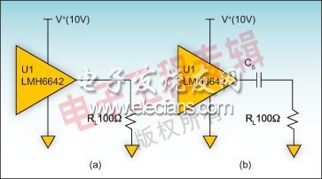

Figure 2: An example of predicting the output voltage swing on a given load.
Consider the application as shown in Figure 2a, where LMH6642 is used to drive a load with RL=100 Ω and connected to Vs/2 (1/2 supply voltage). Suppose that the output of LMH6642 is biased at Vs/2 or 5V in this case:
The question is, can the designer use the LMH6642 data shown in Figure 1 to estimate the possible maximum output swing? The answer is yes.
The question is, can the designer use the LMH6642 data shown in Figure 1 to estimate the possible maximum output swing? The answer is yes.
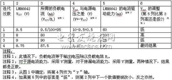

Table 1: Use iteration to predict the output swing of Figure 2a (LMH6642).
Repeat this process until the device characteristics are consistent with the load requirements under the given conditions, and the final result is obtained at the bottom of the second column, thus completing the estimation of swing. Therefore, the repeated results in Table 1 show that the circuit in Figure 2a can produce a maximum voltage of 8.75V on a load of 100 Ω. The converted peak value is 7.5VPP {=(8.75-5) V x 2=7.5VPP}.
Some precautions for the method used in Table 1 are listed below: for the circuit in Figure 2a, only source current can be provided. Therefore, only Figure 1a is used. In each case, assume the worst temperature in Figure 1 to calculate the value in column 5. The value in the fifth column is read from the figure by taking the value in the fourth column as the y-axis in Figure 1a. The final result in column 2, that is, the value of the fourth iteration, is still an approximate solution, because the value in column 3 (87.5 mA) is still lower than that in column 5 (90 mA). However, the resolution in the figure no longer allows fine-tuning of this result.
Now let‘s make a slight change to the example just discussed. Suppose that the output load of LMH6642 is unchanged, but the signal is AC coupled, as shown in Figure 2b. The method for predicting the output swing is the same as the previous one, but because the AC coupling load can only "see" the swing of the signal, the DC component (bias) of the output voltage is blocked by the AC coupling capacitance, so some entries in the table (column 3) need to be modified. In addition, it should also be noted that the AC coupling load requires the output of LMH6642 to accept and provide current (different from the application that only needs output to provide current in Figure 2a). Therefore, select the smaller value of source current and leakage current characteristics and fill in the fifth column of Table 2.


Table 2: Use iteration to predict the output swing of Figure 2b.
The final result (9.6V) in the second column corresponds to the output swing of 9.2VPP {=(9.6-5) V * 2=9.2Vpp} on the AC coupling load. As expected, it is larger than the value (7.5VPP) in the example of the DC coupling load discussed earlier, because there is no DC load.
The process of estimating swing using these optional output capacity charts is very similar to the example given earlier, and the initial guess value is fine-tuned using repeated methods.
How to measure output parameters
The output parameters in the operational amplifier data manual are usually represented by some figures calculated based on a reasonable number of units. The figures in the data book can be said to belong to the "linear" working area, because they show the typical characteristics under closed-loop working conditions. Of course, most operational amplifiers work under closed-loop conditions, but in some specific applications, they also need to work under open-loop conditions. This means that the operational amplifier cannot keep the voltage difference between the input terminals as 0 as usual. This is because the fast input change requires the output of the operational amplifier to change in a very short time. That is to say, the loop is open and the output changes to the final value. During this period, there will be a large voltage difference between the input terminals. Once the final output value is reached, the input voltage difference will again be reduced to very close to 0V (that is, the output voltage divided by the large open-loop gain of the operational amplifier).
As explained earlier, some operational amplifiers can obviously provide higher current under "open loop" conditions due to their architecture. However, under the stable and normal closed-loop conditions used to maintain a certain amount of voltage swing on a load, the output current capacity must be determined under the condition of very small input over-drive voltage. The input over-drive voltage should be greater than the input offset voltage of the operational amplifier input stage, but it should not be too large, otherwise the current capacity will be affected.
In order to obtain the output characteristic diagram, the manufacturer will use the open-loop or closed-loop structure for measurement. As long as the requirements of input over-drive voltage are followed, the results are the same. As shown in Figure 3a, when measuring the open-loop output current, the output of the DUT is connected to a variable current source (or sink) generator (Go) and powered by dual power supplies.
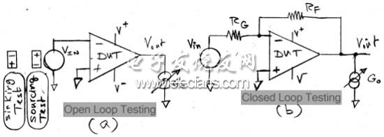

Figure 3: Measured output characteristics.
It is only necessary to apply sufficient differential voltage at the input end to overcome the input offset voltage and "generate" the output (for the test of source current capability, towards the positive power supply; for the test of output well current, towards the negative power supply). This voltage is referred to as the Input Overdrive Voltage (VID). Most operational amplifiers need about 20mV input over-drive voltage to achieve full current output capability. In order to support small output distortion, the input over-drive voltage should be less than+/- 20mV when the output current is specified. Under these conditions, the output current source (current well) generator can scan in an appropriate range and record the output voltage at each scan point. The output characteristic diagram is obtained by drawing the output voltage (directly given or the relationship between the corresponding power supply voltage) and the output current of the corresponding generator on the diagram. If the current source (current well) generator is allowed to provide a large enough current, the output voltage of the final point will be exactly equal to 1/2 of the sum of V+and V - (that is, ground in the system with symmetrical power supply). The current value corresponding to this point is the "output short-circuit current" in the data book, which is usually provided in the data book of most operational amplifiers. As shown in Figure 1, the output short-circuit current is about 100mA, and the corresponding vertical axis coordinate is 5V (for+/- 5V power supply).
The settings in Figure 3b are similar to those in Figure 3a, and can also be used to measure output characteristics. The difference between the two settings is that in the circuit in Figure 3b, the DUT loop is closed by RF and RG. In order to measure the output current capacity under a given VOUT, it is necessary to set an appropriate VIN to obtain the required VOUT. Go will continue to increase until the required input over-drive voltage (VID) is reached (usually less than+/- 20mV, and greater than the input offset voltage, its value can be reduced by VOUT( Δ VOUT). When the values of RF and RG are known, the relationship between input over-drive voltage (VID) and VOUT drop is:
VID=(VOUT/(1+RF/RG), where (VOUT is the change of VOUT caused by the increase of Go
For example, when RF=10K and RG=1K, if Vin=-0.3V, the output will be 3V. The required 20mV input over-drive voltage corresponds to the change of output voltage 220mV {=20mV * (1+10)=220mV} caused by the current change of Go, or VOUT=2.78V.
It is noteworthy that some high voltage swing rate voltage feedback operational amplifiers specially designed for low power applications use a "swing rate enhancement" circuit at the front end. In this way, the operational amplifier can save power consumption and generate high-speed large signal output swing (in other words, high voltage swing). For example, the two high-speed operational amplifiers LM7171 and LMH6657 of National Semiconductor Corporation of the United States. In order to achieve the above purpose, the large input swing increases the current provided to the capacitance of the internal compensation node, which is usually used to limit the swing rate of the operational amplifier. Therefore, the swing rate of such devices is related to the input over-drive voltage.
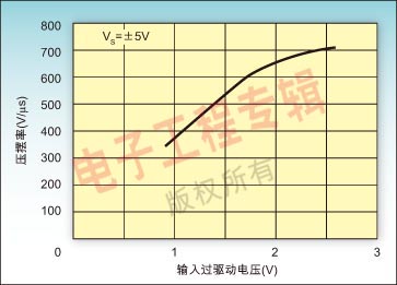

Figure 4: The relationship between the yaw rate of LMH6657 and the input over-drive voltage reflects the enhancement of the yaw rate.
Figure 4 is the function relationship between the yaw rate and the input over-drive voltage given in the LMH6657 data manual.
Therefore, when the input over-drive voltage and output voltage swing rate are large, the output current capacity of such devices is also improved.
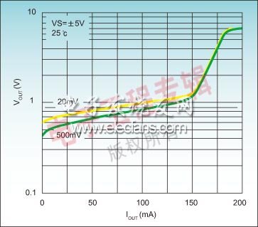
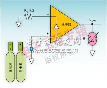

Figure 5: Under two different input over-drive voltages, the output of LMH6657 provides current characteristics.
Figure 5 shows the relationship between the output current supply capacity (IOUT) of LMH6657 and the output voltage under two different input over-drive voltages. It can be seen that the larger input over-drive voltage increases the output current (the figure shows that for the same IOUT, the margin between the output voltage and the power supply voltage is smaller). The accepted current characteristics are not given here, but the results are similar.
Compared with conventional voltage feedback operational amplifiers, it is more necessary to ensure that the output characteristics of such devices are correctly understood. Additional output drive capability can be obtained by increasing the input over-drive voltage. However, when the closed-loop operation with small distortion, such as maintaining a steady swing on the load, requires a small input over-drive voltage (<+/- 20mV). Under the condition that the input overdrive voltage is large, the specified output capacity can only be used for transient behavior. At this time, the output has not reached the final value. Once the output reaches the final value, the input overdrive voltage will drop below 20mV. Therefore, when evaluating the performance of such devices in applications where steady-state output current rather than transient behavior is very important, it is necessary to pay attention to the input over-drive condition.
The measurement method of output characteristics of current feedback (CFB) operational amplifier is very similar to that given above. Figure 6 shows the settings used for this measurement.

Figure 6: Measure the output characteristics of the CFB operational amplifier.
The structure of CFB is composed of a buffer with a gain of 1 between the forward and reverse input terminals. The resistance RG enables the current to flow through the reverse port. If the VIN value is set to be greater than the input offset voltage, the current will flow out of the reverse input port, and the output will grow towards the positive supply voltage V+(that is, it will be as close to V+as possible). As in the case of the voltage feedback (VFB) operational amplifier explained earlier, the current generator Go will scan a series of current values suitable for the DUT to obtain the relationship between the output current supply capacity and the output voltage. By reversing the polarity of the VIN and setting Go to provide current to the output pin of the DUT, the current acceptance ability can be determined. Note that for CFB structure, the influence of input over-drive voltage on output characteristics is smaller than that of VFB structure.
Macro model of output capacity and operational amplifier:
The Pspice macro model provided by National Semiconductor Corporation of the United States to users can well predict many parameters of the operational amplifier, and the output characteristic is one of them. For LMH6642 we have been discussing, Figure 7 shows the output characteristics predicted by the Pspice model of National Semiconductor Corporation of the United States.
When building the Pspice macro model, we try to make the model curve shown in Figure 7 conform to the typical device characteristics shown in Figure 1. However, careful observation will reveal that,?
The curve in Figure 7 is still too idealistic compared with the typical characteristic curve in Figure 1. For the parameters we are trying to model, the Pspice macro model can only provide "limited" accuracy. In addition, in general, the output current model of Pspice does not include the effect that excessive input over-drive voltage in the devices with built-in voltage swing rate enhancement characteristics will enhance the output drive capability.
As long as this behavior is included in the macro model of the operational amplifier, Pspice simulation can directly and quickly estimate the output voltage swing on a series of resistive loads (rather than the output capability shown in Figure 7). When LMH6642 operates under the circuit conditions shown in Figure 1A, the Pspice simulation file shown in Appendix B is a feasible method to obtain the maximum output swing on a series of resistive loads (the resistance range is 60~100 ohms, and the step size is 10 ohms). Figure 8 shows the result graph generated by Pspice.
From this figure, the designer can directly read the output voltage swing of the specified different loads, and draw the relationship diagram between swing and load as shown in Figure 9. For a 100 ohm load, compare the 9.48V swing predicted by Pspice (as shown in Figure 9) with the 8.75V swing predicted by the previous iteration analysis (as shown in Table 1). When comparing the results of Pspice with the typical specifications on the data sheet, a gap of about 8% is common.
|
Disclaimer: This article is transferred from other platforms and does not represent the views and positions of this site. If there is any infringement or objection, please contact us to delete it. thank you! |


