DC/DC Working Principle and Chip Details of Power Supply Design
Time:2022-11-12
Views:1569
DC/DC power supply refers to the power supply converted from DC to DC. From this definition, LDO (low dropout linear regulator) chip should also belong to DC/DC power supply, but generally it only converts DC to DC, and the power supply realized by switching is called DC/DC power supply.
1、 Working principle
To understand the working principle of DC/DC, you must first understand a law and the three basic topologies of switching power supply (do not think that the basic topology of switching power supply is very difficult, you can continue to look down).
1. Volt second balance law of inductance voltage
The working state of a power converter when the input, load and control are all fixed values is called steady state in switching power supply. In the steady state, the inductance in the power converter meets the volt second balance law of the inductance voltage: for DC/DC power converters that have been operating in the steady state, the forward volt second added to the filter inductance when the active switch is turned on must be equal to the reverse volt second added to the inductance when the active switch is turned off.
Do you think it is a little difficult to understand, and then look at the formula derivation process.
Calculation process of volt second balance equation:
The basic equation of inductance is: V (t)=L * dI (t)/dt, that is, the voltage at both ends of the inductance is equal to the inductance inductance multiplied by the change rate of the current passing through the inductance with time.
According to the above equation, dI (t)=1/L π V (t) dt can be obtained. For a power converter in steady state, it should ensure that the energy charge and discharge in the inductance are equal in a cycle, which is reflected in the V-t diagram, that is, the sum of its areas in a cycle is 0, so the volt second balance law of the inductance voltage can be obtained. Here you can refer to: Page 8 of DC/DC Power Details (if you cannot understand it here, you can first read the working principles of the following three basic topologies of switching power supply).
Extended data:
1. When an inductor suddenly adds a voltage, the current in it gradually increases, and the larger the inductance, the slower the current increases;
2. When the current on an inductor is suddenly interrupted, an instantaneous high voltage will be generated at both ends of the inductor, and the greater the inductance, the higher the voltage;
3. The basic equation of capacitance is: I (t)=dV (t)/(C * dt). When a current flows through the capacitance, the voltage at both ends of the capacitance gradually increases, and the greater the capacitance, the slower the voltage increases;
2. Three basic topologies of switching power supply
2.1 Buck step-down type

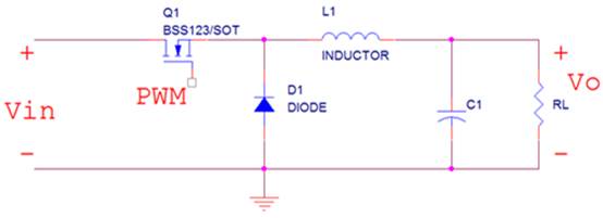
Figure 1 Schematic diagram of BUCK basic topology simplification

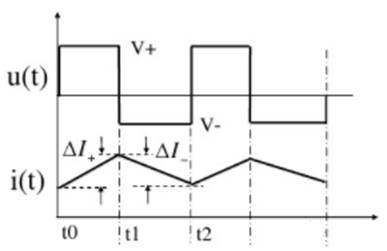
Fig. 2 V-t Characteristic Diagram of Inductance
The basic topology principle of the BUCK type is shown in Figure 1, and the V-t characteristic diagram of its inductance L1 is shown in Figure 2.
When the PWM drive MOS tube Q1 is turned on, the conduction voltage drop of MOS tube is ignored. At this time, the voltage at both ends of the inductor remains unchanged as Vin Vo. According to the basic equation of the inductor: V (t)=L * dI (t)/dt, the inductance current will rise linearly. At this time, the forward volt second of the inductor is: V * Ton=(Vin Vo) * Ton.
When the PWM drives MOS transistor Q1 to the end, the inductance current forms a loop through the freewheeling diode D1 (ignoring the diode voltage drop), and the inductance current does not change abruptly. Similarly, the voltage at both ends of the inductance remains unchanged as Vo, the direction is opposite to (Vin Vo), and the inductance current decreases linearly. At this time, the reverse voltage second of the inductance is: V * Toff=Vo * (Ts Ton), and Ts is the PWM waveform period.
According to the volt second balance law of inductance voltage, we can get: (Vin Vo) * Ton=Vo * (Ts Ton)
Vo=D * Vin (D is the duty cycle)
2.2 BOOST booster type

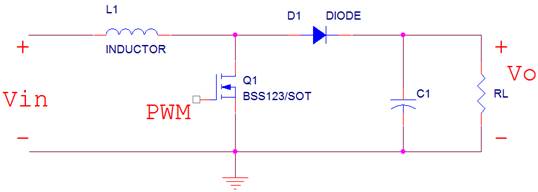
Figure 3 Schematic Diagram of BOOST Basic Topology Simplification
Figure 3 is a simplified schematic diagram of BOOST boost type basic topology. Its analysis method is similar to that of BUCK circuit.
When the PWM driving MOS tube is turned on, the positive volt second of the inductance is: Vin * Ton;
When the PWM drives the MOS tube to the end, the reverse volt second of the inductance is: (Vo - Vin) * (Ts Ton).
According to the volt second balance law of inductance voltage, Vin * Ton=(Vo - Vin) * (Ts Ton)
Vo=Vin/(1-D)
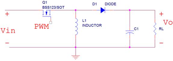
2.3 Buck-BOOST polarity reversal voltage up and down type (diode direction in this circuit is reversed)

Fig. 4 Simplified working principle diagram of BUCK-BOOST basic topology
The BUCK-BOOST circuit analysis method is the same as the above two types of basic topology analysis methods. When the MOS tube is turned on, the forward volt second of the inductor is: Vin * Ton; When MOS tube is cut off, the reverse volt second of inductance is: - Mo * (Ts Ton).
According to the volt second balance law of inductance voltage, we can get: Vin * Ton=- Mo * (Ts Ton)
Vo=- Win * (D/(1-D))
Extended data
1. The DC/DC power supply chip mainly adjusts the duty cycle of the driving waveform of MOS transistors by comparing the feedback voltage with the internal reference voltage to ensure the stability of the output voltage.
2. Synchronous rectification technology
As there is more or less tube voltage drop when the diode is turned on, the power consumed by the freewheeling diode will become the main power consumption of DC/DC power supply, which severely limits the improvement of the efficiency of the DC/DC power supply chip. In order to solve this problem, MOS tube with very small conduction resistance is used to replace the freewheeling diode, and then the controller controls the switch tube and synchronous rectifier tube at the same time. To ensure that the two MOS tubes cannot be connected at the same time, it is responsible for short circuit.
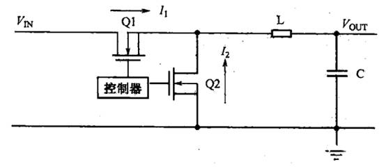
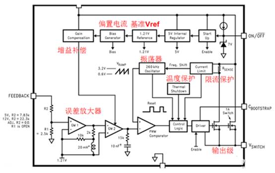

Figure 5 Buck circuit with synchronous rectification
2、 DC/DC power modulation mode
The DC/DC power supply belongs to the chopper type, that is, according to a certain modulation mode, the high-speed switch is continuously turned on and off, and the DC power level can be converted by controlling the on-off duty cycle of the switch. There are three modulation modes for DC/DC power supply: PWM mode, PFM mode, and the mixed mode of PWM and PFM.
1. PWM (pulse width modulation)
PWM adopts constant switching frequency, and achieves stable power supply voltage output by adjusting the pulse width (duty cycle). In PWM modulation mode, the switching frequency is constant, that is, there is no case of being turned off for a long time.
Advantages: low noise, high efficiency, fast response to load changes, and support continuous power supply mode.
Disadvantages: The aging rate of light load is low, and the circuit is unstable, so false load is required in design.
2. PFM (pulse frequency modulation)
PFM can achieve stable output of power supply voltage by regulating switching frequency. When PFM is working, its output will be turned off when the output voltage exceeds the upper threshold voltage, and it will not work again until the output voltage falls below the lower threshold voltage.
Advantages: low power consumption, high efficiency and no need to provide false load when the load is light.
Disadvantages: slow response to load changes, relatively large output voltage noise and ripple, not suitable for continuous power supply mode.
3、 Internal structure of DC/DC chip
Next, let‘s take a look at the unit modules inside the DC/DC power supply chip, and show you the relationship between the basic topology and the power supply chip. First, let‘s look at a diagram.

Fig. 6 Internal composition of DC/DC power supply chip
1. Error amplifier: The function of the error amplifier is to amplify the difference between the feedback voltage (FB pin voltage) and the reference voltage, and then use the signal to control the duty cycle of the PWM output signal.
2. Temperature protection: When the temperature is higher than the limit value, the chip stops working.
3. Current limiting protection: if the current on the resistance of the current comparator is too large, the output will decrease until the lower threshold value is exceeded, and the power chip will have hiccups. This mode can protect the chip and the voltage regulator in case of short circuit in the output. Once the over-current phenomenon is eliminated, the hiccup will also be eliminated.
4. Soft start circuit: It is used to reduce the surge current when the power is started, so that the output voltage rises slowly, reducing the impact on the input power.
4、 Selection criteria for hardware design parameters of DC/DC circuits
1. Set the output voltage: select the appropriate R2 first. If R2 is too small, the static current will be too large, resulting in increased loss; If R2 is too large, the quiescent current will be too small, which will cause the feedback voltage of FB pin to be sensitive to noise. Generally, there is a recommended value range in the datasheet. Select R2, calculate the value of R1 according to the output voltage, R1=((Vout Vref)/Vref) * R2.
2. Inductance: the inductance shall be selected to ensure that the inductance current remains continuous until the minimum specified current is output. In the process of inductor selection, it is necessary to comprehensively consider the output current, ripple, volume and other factors. A larger inductance will lead to a smaller ripple current, resulting in a lower ripple voltage. However, a larger inductance will have a larger physical footprint, higher series resistance, and lower saturation current. Generally, there will be corresponding calculation formulas in the chip datasheet.
3. Output capacitance: The selection of output capacitance is mainly based on the requirements of output ripple required in the design.
Ripple generated by capacitance: relatively small, negligible;
Ripple generated by capacitance equivalent inductance: below 300KHz~500KHz, can be ignored;
Ripple generated by capacitor equivalent resistance: it is proportional to ESR and the current flowing through the capacitor. The current ripple is mainly related to the switching frequency of the switch tube, which is basically the nth harmonic of the switching frequency. In order to reduce the ripple, the ESR should be as small as possible.
|
Disclaimer: This article is transferred from other platforms and does not represent the views and positions of this site. If there is any infringement or objection, please contact us to delete it. thank you! |


