Bridging Method of Class D Power Amplifier IC
Time:2022-10-29
Views:1673
Compared with traditional Class A, Class B or Class AB linear amplifiers, Class D audio amplifiers have many advantages. Linear amplifiers can have higher efficiency at very low signal levels, depending on how they are biased. However, as the output signal level increases, this advantage disappears, and Class D amplifiers perform better. According to the design, Class D amplifiers can have higher idle power consumption due to switching losses in their output devices. Due to the core loss of the output inductor and the ESR loss of the output filter capacitor, they will also suffer parasitic losses in the output LC filter. But even with these limitations, in most applications and typical music duty cycle, the average efficiency of Class D amplifier in power consumption is about twice that of it. From the perspective of component counting, they are not so complex; Requires less heat dissipation and less power. They also pack more compactly, which can reduce the cost, because it is possible to cut the heat capacity of the system in half.


This article will focus on the use of Class D solutions in bridge mode.
The standard configuration for Class D solutions is a half bridge output stage. The bridge or full bridge operation uses two standard half bridge channels to form a floating bridge type tie down output. When working in the bridge mode, one end of the load is connected to the half bridge in-phase output, and the other end is connected to the non electric half bridge amplifier. In this way, the positive rail at one end of the load and the negative rail at the other end modulated by the incoming signal alternate with the polarity of the signal source. In many applications, it is advantageous to use a Class D full bridge configuration. Full bridge operation allows full utilization of the total supply voltage available. For the same total power supply voltage, the bridged load or BTL connection generates twice the voltage swing to the load. It also provides better power supply noise rejection or PSRR, power supply rejection ratio. Finally, it makes it easier for the end user to connect the amplifier to a unipolar power supply without having to output DC blocking capacitors, and may save the designer costs and the complexity of the bipolar power supply, which is required for half bridge operation. In many designs, when the supply voltage is limited, the use of BTL amplifiers can maximize the available power to the load.
At the other end of the voltage spectrum of the high-voltage direct drive system or ultra-high power design, having twice the output voltage swing can avoid the need for high-voltage MOSFETs, gate drivers and or boost matching transformers. This may be a considerable audio performance and efficiency advantage, because the quality of audio switching devices decreases with breakdown voltage. In addition, very high voltage switching amplifiers may require output inductors, corresponding high voltage second products and low hysteresis losses.
All these show that this circuit topology has some disadvantages, because it requires twice as many semiconductor components, which increases the cost and complexity of this method. Other disadvantages include slight loss of efficiency in the whole output power range, because the switching loss and conduction loss are doubled. This topology also requires two output inductors, which brings additional costs and the cost of PCB space. In this article, we will discuss in detail the relative advantages and disadvantages of half bridge and full bridge operation of Class D audio amplifiers.
One of the greatest advantages of full bridge operation is that the power supply voltage can be fully utilized. The output voltage swing is about twice that of half bridge mode. If you do a simple mathematical operation on the same load impedance, you will get four times the power because it is proportional to the square of the output voltage. We refer to this mode of operation as BTL or bridge load to avoid confusing the rest of this document. Another advantage of BTL operation is that it greatly improves the power interception rate. This means that the noise and voltage ripple existing in the power track are rejected at a higher rate. Before negative feedback is applied to the whole circuit in many BTL amplifiers, the open loop of PSRR is close to 60db. With the closing of the negative feedback loop, there will be additional improvements, depending on the loop gain that exists in the design. For example, at 1 KHz plus an additional 40 dB loop gain, the PSRR will be around 100 dB.
Another common phenomenon in half bridge topology is called "bus pumping". When the output energy of the load and LC output filter returns to the power rail of the amplifier, compared with no signal, bus pumping occurs. In fact, when there is little storage capacity or very low frequency load energy is returned to the power supply, the voltage may increase by more than 10 volts on both the positive and negative poles. This effect can be minimized by using very large filter capacitors on the track, but it will not eliminate this effect, especially at lower audio frequencies. BTL mode eliminates this problem because half of the output stage is source current and the other half is sinking current, so this situation is effectively cancelled.
Another advantage of BTL operation is that it can operate on a unipolar power supply. This eliminates half of the large energy storage capacitors on the high voltage bus, which can save a lot of money in terms of cost, space and circuit complexity. Another advantage is that the output DC offset between the two active outputs is close to zero. When using this power configuration to operate the half bridge topology, it is not necessary to add a large output coupling capacitor to prevent any DC from flowing through the load.
A major disadvantage of BTL topology is that its implementation requires twice the number of active components. This means that the number of gate drivers and output devices must be used at least twice. Of course, this increases the cost, space, and complexity of the circuit. Therefore, we may save design costs in the power supply part, which will increase in the output stage and the output LC filter module. This is exactly what we call "borrowing while repaying".
Depending on the power level of the amplifier, this may mean increasing the cost of the entire system. Another disadvantage is that the efficiency of the BTL solution is slightly reduced, because if the number of active output components is doubled, the switching loss and conduction loss will be doubled. Passive output filter usually uses two inductors in BTL, so the core loss and I ² R Copper loss will also be doubled. However, for the same output power level as the half bridge topology design, the voltage swing between each inductor is half, so the core loss of each inductor may be less than half.
When we convert Class D amplifier from traditional half bridge to BTL operation, we need to pay attention to some design considerations. Because the load of the output stage can be driven by double voltage swing at both ends, the reflected load impedance of each amplifier is only half of its original size. In order to recover to the original half bridge working power level under the same power bus voltage, the load impedance must be increased by four times. With the load impedance unchanged, the power supply voltage needs to be halved to maintain the same power output rating. Finally, the value of the passive output filter needs to be adjusted accordingly to maintain the same load output frequency response. Finally, based on the phase when the output is idle again, there are two different BTL operation modes, AD like (Class AD) or BD like (Class BD). In short, when AD is idle, it outputs PWM waveform in the opposite direction, while BD outputs the opposite result. These two different modulators will have the opportunity to discuss in the future. In the next section, we will discuss any special considerations in LC output filter and BTL design starting with half bridge synthesis. For completeness, it includes classes AD and BD.
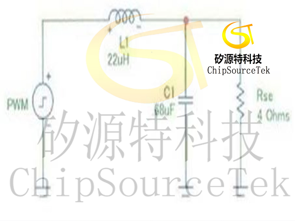
Standard second-order low-pass filter for single ended design:

Fig. 1 Single ended LC output filter with standard value Q=0.707 RL=4 Ohms Fc=40 KHz
EQ1 represents the transfer function of half bridge Class D single ended second-order low-pass filter:
H(s) = Vo / Vi = (1/sL) / (1/sL + sC + (1/R): (EQ1), C = Q / w0RL , L = RL / Qw0 and Q = RL(C/L)1/2
Where w0=cut-off frequency of the filter in radians/second=1/(LC) 1/2
We define W as (w0) ²; Substitute W and Q into the transfer function to get EQ2:
H(s) = W / (s2 + s ( ω 0 / Q) + ( ω 0)2 ) = (1/LC) / (s2 + s / (RLC) + (1/LC)):(EQ2)
At the cut-off frequency, ω = ω 0, ( ω 0=2 π FC, FC=filter cut-off frequency Hz), the output filter will be heavily damped at Q=0.707, and then considered as "maximum smoothing".
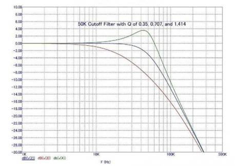
When the Q value is ≥ 0.707, the output filter will have a peak value. The typical frequency response of the output filter under different Q values is shown in the figure below.

Figure 2 Q Value of Frequency Response VSLC Output Filter
Because the typical IR Class D amplifier design does not include an output LC filter in the feedback loop, the overall frequency response of the circuit will change significantly as the load impedance changes. The output filter usually aims to produce the minimum peak at high frequency, but in some cases, 1 or 2 dB of a small amount of peak at 20KHz is acceptable, especially that most people cannot hear 15KHz, and higher Q output filter may cause more output voltage ripple attenuation at the switching frequency. In general, it is feasible to achieve at least 40 dB or more attenuation at the average switching frequency of the amplifier. The IR class D circuit is self oscillating, so its switching frequency can vary in a fairly wide range. The target switching frequency of most designs is about 400 khz. Therefore, in order to achieve 40db (100X) switching ripple attenuation using a second-order filter, the cut-off frequency should be reduced by about 10 times, typically 40 khz. The ideal output filter should be as flat as possible and exhibit the frequency characteristic of Butterworth "critical damping". If the phase linearity is important, the minimum phase filter, such as Bessel filter, can be used, but it will bring a drooping frequency response to the high frequency response, depending on the position of the filter cut-off frequency.
The selection of the output inductor is critical, which not only affects the total harmonic distortion of the amplifier, but also affects the efficiency of the amplifier. As mentioned earlier, the output filter is not included in the feedback loop, so any nonlinearity in the inductance will directly affect the performance of the amplifier. Its core loss is also crucial to the efficiency of the design, because even in the idle Class AD design, a high-voltage and high-frequency square wave with a duty cycle of 50% will pass through it. If the core material is not carefully selected, the output inductor will emit a lot of heat, which will lead to high operating temperature of the filter element and high idle power loss. In some cases, this choice is unwise, and these parts may actually be very hot. In many cases, the best core material is interstitial ferrite because of its low core loss and excellent linearity.
|
Disclaimer: This article is transferred from other platforms and does not represent the views and positions of this site. If there is any infringement or objection, please contact us to delete it. thank you! |


