How can you improve your dynamic loop response
Time:2022-10-05
Views:1716
The DC-DC converter converts the changing input voltage into (usually) a fixed output voltage through a feedback control system. The feedback control system shall be stable as far as possible to avoid oscillation or the worst case: output of unregulated output voltage. The speed of the control system shall be as fast as possible to respond to dynamic changes, such as rapid input voltage changes or load transients at the output terminals, and minimize the output voltage deviation after regulation. To show the behavior of the control loop, a typical Bode diagram can be used to show the changes of the phase shift and gain of the loop with frequency. This control loop can be realized by analog or digital technology.
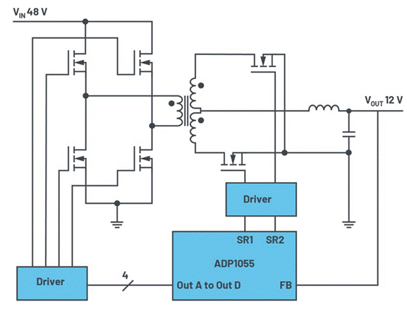
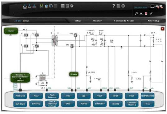
Some digital power supplies provide control loop optimization and can respond to dynamic effects very quickly. Figure 1 shows the circuit example of ADP1055 controller IC, which has digital control loop optimization function. Digital controllers provide designers with many control functions, some of which can be dynamically controlled even during operation. Figure 2 shows the various ADP1055 functions that can be controlled by the ADP1055 evaluation software.

圖1. ADP1055數(shù)字開關(guān)穩(wěn)壓器的全橋應(yīng)用。

Figure 2. Digital power supply enables designers to easily manage power parameters through a graphical user interface.
The non-linear gain/response function provides a very interesting setting option related to the control loop, which is accessed via the filter button. Nonlinear gain/response supports dynamic control loops, such as dynamic adjustments immediately after load transients. After a great load transient, the output voltage of the power supply usually fluctuates around the ideal rectifier voltage. In the control loop that only uses analog devices, selecting the control loop and power level devices of the power supply can minimize the fluctuation of the voltage under most expected conditions. The advantage of a digital adjustable control loop (such as a feature in ADP1055) is that the response of the loop can be adjusted to achieve compensation in various situations with large differences.
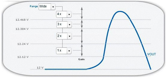
Figure 3 shows the interface that controls this function. The blue curve in the figure shows the typical behavior of the output voltage after the load transient from high to low. It can be seen that the voltage response at the output end of the voltage regulator will usually overshoot. When the output voltage exceeds some thresholds, the overshoot can be minimized by simply increasing the control loop gain.

Figure 3. Set the control loop gain according to the output voltage state.
In the example of Figure 3, the nominal output voltage is set to 12 V. The adjustable control loop gain can be set to multiple values, depending on the output voltage. For example, if the voltage rises above 12.12 V due to the gain increase of the error amplifier, you can set the control loop in the corresponding pull-down menu. There are three other voltage thresholds above 12.12 V, which can be set independently of the gain. Note that these gain settings are completely independent of the poles and zeros set when designing the voltage stabilizing loop.
The adjustable voltage based gain setting can find the control loop setting that responds to voltage overshoot more quickly, thus optimizing the quality of output voltage feedback control. Note that the optimized control loop characteristics will not be affected during normal operation. Digital controllers (such as ADP1055) can be used to dynamically adjust the control loop under specific conditions (such as after experiencing load transients), but it is difficult to achieve with traditional analog control loops.
ADP1055
·Operating temperature range − 40 ° C to+125 ° C, EEPROM data retention period at 125 ° C is 15 years
·Compatible with PMBus revision 1.2
·32-bit password protection with command mask
·64 address options (16 base addresses, expandable to 64)
·6 PWM control signals, 625 ps resolution
·Duty cycle double update rate
·Digital control loop (PID+additional pole or zero configurable capability)
·Programmable loop filter (CCM, DCM, low temperature/normal temperature)
·Frequency synchronization
·Soft start and soft stop functions
·Average and peak constant current mode
·External PN junction temperature detection
·4 GPIOs (2 GPIOs can be configured as active clamp PWM)
·Fast line voltage feedforward
·Adaptive dead time compensation for efficiency optimization
·Expand black box data recording capabilities to record faults
|
Disclaimer: This article is transferred from other platforms and does not represent the views and positions of this site. If there is any infringement or objection, please contact us to delete it. thank you! |


