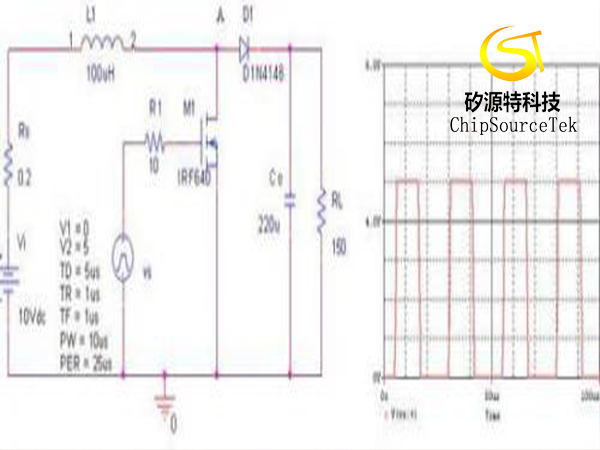
Principle of boost circuit
Time:2022-02-21
Views:2421
Generally, the switch Q1 turns on the inductive energy storage and the capacitor C supplies power. After the switch M1 is closed, the left negative right positive electromotive force is generated to turn on the diode and supply power.
Boost conversion is generally also called boost conversion. Inductor L stores energy and realizes the purpose of boost through the on and off of M1.

Boost boost circuit
AA voltage is low, and the bottleneck of flyback boost circuit restricting power and efficiency lies in switch, rectifier and other losses (including inductance)
1. The inductor shall not be too small (unable to store due energy) or too small wire diameter (large pulse current will cause large wire loss)
2.Most rectifiers use Schottky, which is the same as everyone. When the output is 3.3V, the rectification loss is about 10% 3 switch tube, the key here, put a large amount of enough into saturation, and the conduction voltage drop must be small, which is the key to success The total voltage is only one volt. If there is too much consumption on the pipe, there will be no electricity. Therefore, the pipe voltage drop should be no more than 0.2-0.3v when the maximum current is selected. If it is impossible to do it alone, multiple pipes will be connected in parallel
4 what is the maximum current? Let‘s be simple. It‘s more than that Due to the low efficiency, it will exceed 1.5A, which is the average value. It is 3a in half cycle power supply, and the actual current waveform is 0 to 6A So I suggest that we should use two pipes called 5A and 3a together to deal with it
5.The ready-made chips do not integrate the tubes with such a large current, so I suggest using native circuits is enough for foreign circuits
When the switch is on, the power supply forms a loop through the inductor switch, and the current is converted into magnetic energy in the inductor for storage; When the switch is turned off, the magnetic energy in the inductor is converted into electrical energy, which is negative on the left and positive on the right at the inductor end. This voltage is superimposed on the positive end of the power supply and forms a loop through diode load to complete the boost function. In this case, to improve the conversion efficiency, we should start from three aspects:
1. Reduce the impedance of the circuit when the switch is turned on as much as possible to convert electrical energy into magnetic energy as much as possible;
1. Reduce the impedance of the circuit when the switch is turned on as much as possible to convert electrical energy into magnetic energy as much as possible;
2.Reduce the impedance of the load circuit as much as possible, so that the magnetic energy can be converted into electrical energy as much as possible, and the loss of the circuit is the lowest;
3. Reduce energy consumption as much as possible, because it is meaningless for circuit conversion and cannot supply energy.
|
Disclaimer: This article is transferred from other platforms and does not represent the views and positions of this site. If there is infringement or objection, please contact us to delete. thank you! |


